


What is a FET
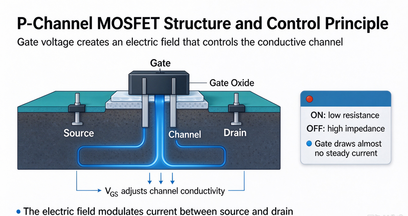
A Field Effect Transistor (FET) is a voltage-controlled semiconductor device. Unlike bipolar transistors (BJT) which rely on input current to turn on, FET works by applying a voltage to the gate terminal. The electric field generated by gate voltage modulates the conductivity of the channel between source (S) and drain (D).
Key feature: The gate draws almost no steady-state current. This gives FET an extremely high input impedance, which is one of its biggest advantages. MOSFET (Metal-Oxide-Semiconductor Field-Effect Transistor) is the most widely used subtype of FET in power supplies, motor drives and battery systems.
FET has two main categories:
- JFET (Junction FET): Early type, normally-on by default. Less common in power circuits today.
- MOSFET: Insulated gate structure. Split into N-channel (NMOS) and P-channel (PMOS). The reverse protection MOS you are studying belongs to PMOS.
Core Functions & Working Principles
1. Electronic Switch (Most important for power MOSFET)
This is the application you focused on: reverse polarity protection, battery power path, BLDC motor drive, DC-DC converters, PFC circuits, LED drivers, battery BMS.
- ON state: Apply suitable gate-source voltage, conductive channel forms between drain and source. D-S resistance becomes very low (Rds(on)), large current can flow with low conduction loss.
- OFF state: Remove gate voltage, the conductive channel disappears. D-S becomes high impedance, almost no current passes through.
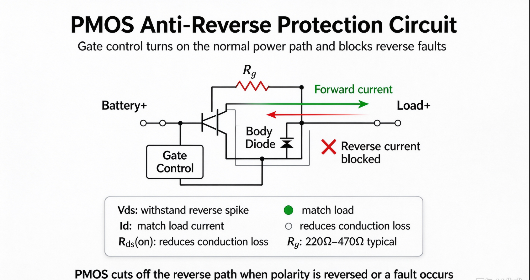
Important note: MOSFET cannot block reverse current by itself. That’s why we use PMOS for anti-reverse circuits, leveraging its body diode and gate control logic. The gate resistor Rg is used to adjust switching speed, suppress oscillation and limit gate surge current. Too large Rg will slow down turn-on / turn-off speed, increase switching loss and weaken noise immunity.
2. Analog Signal Amplification
FET is widely used in low-noise pre-amplifiers, sensor signal conditioning, audio front-end circuits.
When biased in the saturation region, tiny changes in gate voltage will produce proportional changes in drain current.
The ultra-high input impedance ensures the FET will not load down weak signal sources, which is much better than BJT for high-impedance sensors.
3. Voltage-controlled Variable Resistor
When operating in the linear (triode) region and Vds is small, the drain-source resistance can be continuously adjusted by changing gate voltage.
Engineers use this characteristic for signal attenuation, automatic gain control, analog tuning circuits.
4. Constant Current Source / Current Limiter
When working in saturation region, drain current is mostly determined by gate voltage and barely affected by drain-source voltage.
This property can be used to build stable current sources for LED constant current driving and sensor biasing.
5. Fundamental unit for digital ICs
All modern microcontrollers, CPUs, FPGAs are built with billions of NMOS and PMOS forming CMOS logic gates.
CMOS uses paired NMOS/PMOS to represent logic 0 and 1. It consumes almost no static power, which is the foundation of modern digital electronics.
6. Impedance buffer / impedance transformation
The high input impedance and relatively low output impedance make FET an excellent buffer stage.
It isolates the signal source from the rear load, preventing signal attenuation caused by impedance mismatch.
Key MOSFET Parameters to pay attention to
- Vds: Maximum drain-source voltage rating
- Id: Continuous drain current rating
- Rds(on): On-resistance, determines conduction heat loss
- Vgs(th): Gate threshold voltage
- Qg: Total gate charge, determines switching speed and drive power requirement
- Body diode: Intrinsic diode between drain and source, critical for anti-reverse and synchronous rectifier design
Common Limitations
- Gate has parasitic capacitance (Cgs, Cgd, Cds). When switching high speed, gate charge needs to be charged/discharged, requiring transient gate current.
- Gate oxide layer is thin and sensitive to electrostatic discharge (ESD). Static voltage can break the gate easily.
- Rds(on) rises with temperature. When the MOS gets hot, conduction loss increases further.
- Parasitic inductance from packaging and PCB layout may cause voltage spike and oscillation during fast switching.


-

MOSFET type and construction
-

Ultimate Guide to MOSFET Power Amplifiers: Unde...
-

MOSFET Selection | N-Channel MOSFET Constructio...
-

Small Signal Model MOSFET Analysis and Implemen...
-
Commonly used SMD MOSFET package pinout sequenc...
-

How to determine the high-power MOSFET is burne...
-

Recognition of Insulated Layer Gate MOSFETs
-

How Much Current Is Required to Drive a MOSFET?
-

Did you know about the evolution of MOSFET?
-
How Enhanced Package MOSFETs Work
-

Parallel Theory of MOSFETs and Transistors
-

What is PMOSFET, do you know?
-

Characteristics of Enhanced MOSFETs
-

High Voltage Gate Drivers: Powering Next-Genera...
-

Fast Switching MOSFETs: The Complete Guide to N...
-

Basic Requirements for MOSFET Driver Circuits


