


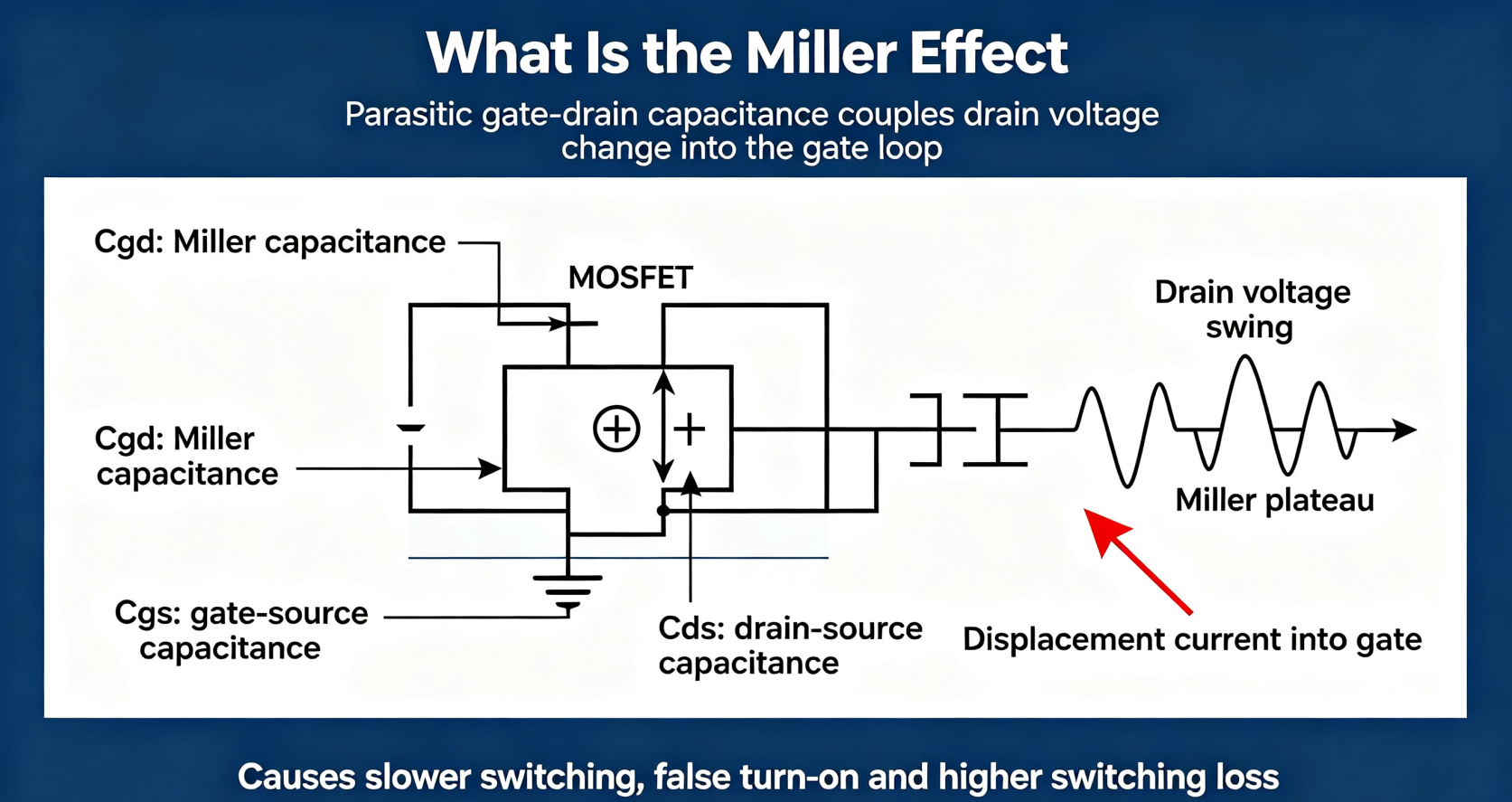
We cannot completely erase the physical Miller capacitance, so the goal in engineering is suppress, not fully eliminate.
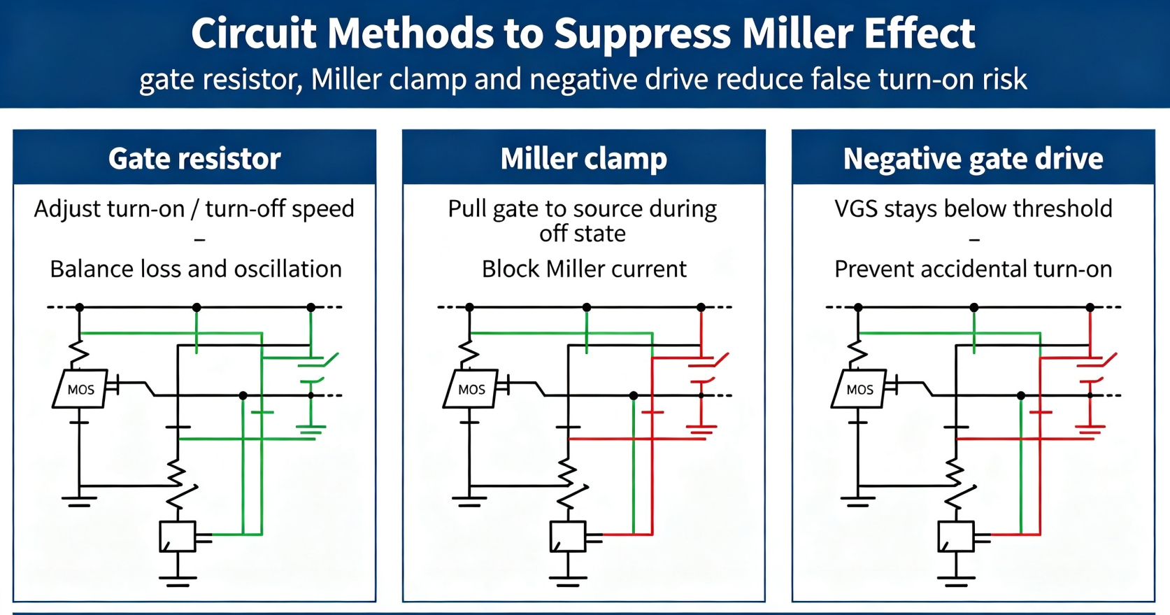
1. Gate‑resistor optimization (most commonly used method)
Add appropriate gate resistor Rg in series to the gate driving loop. It changes gate charging / discharging speed, suppresses the current spike caused by Miller capacitance.
1.2 Usage
- Increase Rg: suppress Miller plateau oscillation, reduce EMI, but switching loss will rise.
- Reduce Rg: faster switching, lower switching loss, but aggravate Miller oscillation and risk of false turn‑on.
1.3 Practical tip
Do not use too large Rg. Split into two resistors: one resistor for turn‑on, another smaller resistor plus diode for turn‑off, to separate turn‑on / turn‑off driving strength. This balances loss and anti‑Miller performance.
2. Add Miller clamp (gate clamp)
Add a dedicated clamp transistor or simple diode‑clamp circuit between gate and source. When Miller current injects to gate, the clamp pulls gate voltage firmly down to source potential, preventing false turn‑on.
2.2 Typical scenario
Half‑bridge / LLC circuits, where the lower MOS may be falsely turned‑on by Miller effect from upper‑tube switching. Many dedicated gate‑driver ICs integrate internal Miller‑clamp pin.
2.3 Advantage: Very effective against parasitic false turn‑on; does not greatly sacrifice switching speed.
3. Use gate‑drive power supply with negative voltage
Drive MOSFET with negative gate‑source voltage (‑5V ~‑8V) when turning off. Even if Miller current injects charge to gate, the gate‑source voltage still stays well below MOS threshold voltage, avoiding accidental turn‑on.
3.2 Application
High‑power half‑bridge, full‑bridge, SiC MOS power converters.
3.3 Disadvantage: Need extra negative power rail, increases circuit complexity and BOM cost.
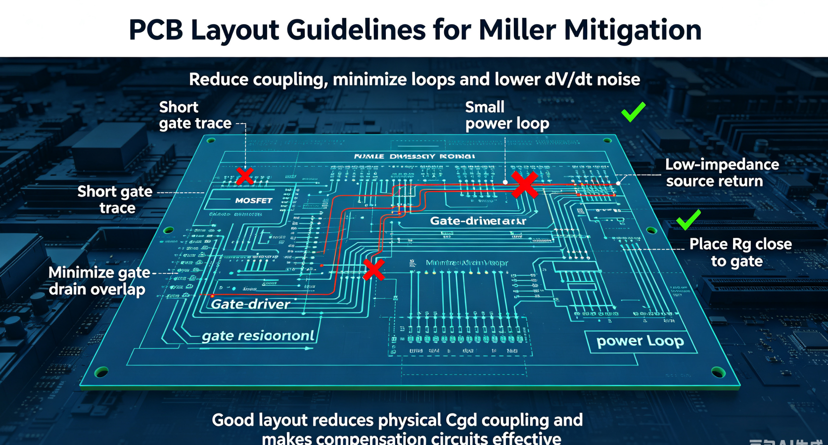
4. PCB layout optimization (critical hardware measure)
Shorten gate trace length; reduce overlapping area between gate trace and drain power copper, to lower physical parasitic Cgd coupling on PCB.
4.2 Reduce gate‑source loop impedance
Place gate‑resistor and gate‑driver IC close to MOSFET gate‑source pin. Keep gate‑source return path very short. Low‑impedance source path can quickly absorb Miller displacement current.
4.3 Power‑loop minimization
Make high‑current power loop as small as possible, suppress drain‑voltage sharp overshoot, reduce the amplitude of voltage change dV/dt, which is the source of Miller current.
5. Device‑level selection
5.2 For high‑frequency hard‑switching applications, prefer trench‑gate or shield‑gate SGT MOS; SiC MOS also has different Miller‑charge characteristics compared with silicon MOS.
Note: You cannot remove Cgd completely; you can only pick devices with better parameters.
6. Active Miller clamp built‑in driver IC
6.2 This removes requirement for negative power supply, widely used in LLC, PFC, motor‑drive circuits.
7. Common misconceptions
7.2 ❌ Simply increasing gate resistance infinitely is not good. Excessive Rg will sharply raise switching loss and temperature.
7.3 ❌ Only focus on peripheral circuit and ignore PCB layout. Bad layout will make all peripheral compensation circuits ineffective.
8. Quick selection guide for engineering
8.2 Half‑bridge / LLC power supply: Use driver IC with integrated active Miller clamp.
8.3 High‑power industrial / SiC application: Active clamp + negative gate drive + optimized power loop.
Summary
- Miller effect stems from MOS parasitic gate‑drain capacitance, cannot be completely eliminated.
- Main suppression means: gate resistor adjustment, Miller clamp, negative turn‑off voltage, optimized PCB layout, selecting low‑Qgd MOSFET.
- For half‑bridge topology, active Miller clamp is one of the most cost‑effective solutions.


-

Floating Gate MOSFET Implementation: Key Steps ...
-

MOSFET Classification Characteristics
-

Understanding MOSFET Transconductance: Essentia...
-
Introduction to the working principle of common...
-

Impact of Sustained Extreme Heat in India on th...
-

Testing MOSFETs with a Multimeter: Essential St...
-

Special Circuit Design for Power Amplifiers Usi...
-

New MOSFET Sourcing Choice: WINSOK Domestic Sub...
-

2N7002 LTspice Modeling and Simulation Guide
-

A Comprehensive Guide about What is VGS in MOSFET
-
What is a MOSFET? What are the main parameters?
-

Discrete MOSFETs: Powering Tomorrow’s Ele...
-

The importance of power MOSFET in motherboard d...
-

MOSFET as Ideal Diode: Revolutionary Approach t...
-
How to correctly select small voltage MOSFETs
-

Working with MOSFETs: Essential Knowledge for E...


