
- MOSFET Selection Parameters
- Core selection priority: Breakdown Voltage, Drain Current, On-resistance, Gate Charge, Threshold Voltage, Package & Thermal Resistance
- 1. Absolute Maximum Ratings
- 1.VDSS: Drain-source breakdown voltageReserve 1.5~2x margin over actual operating voltage to avoid breakdown.
- 2.ID: Continuous drain currentDerate to 50%~70% under high temperature; take 1.5~2x rated value for safety.
- 3.IDM: Peak pulsed drain currentSustain surge current from inductive loads and instant startup.
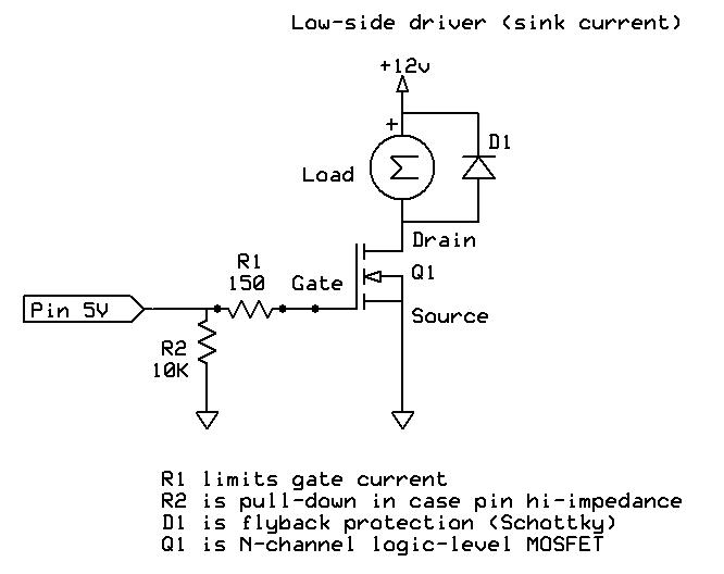
- 4.VGS: Gate-source voltageCommon range: ±20V; logic-level MOSFET: ±12V.
- 5.PD: Maximum power dissipationActual working power shall not exceed 80% of rated power.
- 2. Static Characteristic Parameters
- 1.RDS(on): Drain-source on-resistanceLower value brings less conduction loss and heat generation.
- 2.VGS(th): Gate threshold voltageStandard type: 2~4V; Logic type: 1~2.5V for direct MCU driving.
- 3. Dynamic Characteristic Parameters
- 1.Qg: Total gate chargeSmaller value achieves faster switching speed and lower drive loss.
- 2.Ciss/Cgs/Cgd: Input & parasitic capacitanceCritical index for high-frequency circuit design.
- 3.tr/tf: Rise & fall timeShorter time reduces switching loss.
- 4. Thermal Parameters
- 1.Tj: Junction operating temperatureNormal range: -55℃ ~ 150℃.
- 2.RθJC/RθJA: Thermal resistanceSmaller thermal resistance means better heat dissipation.
- 5. Package & Channel Type
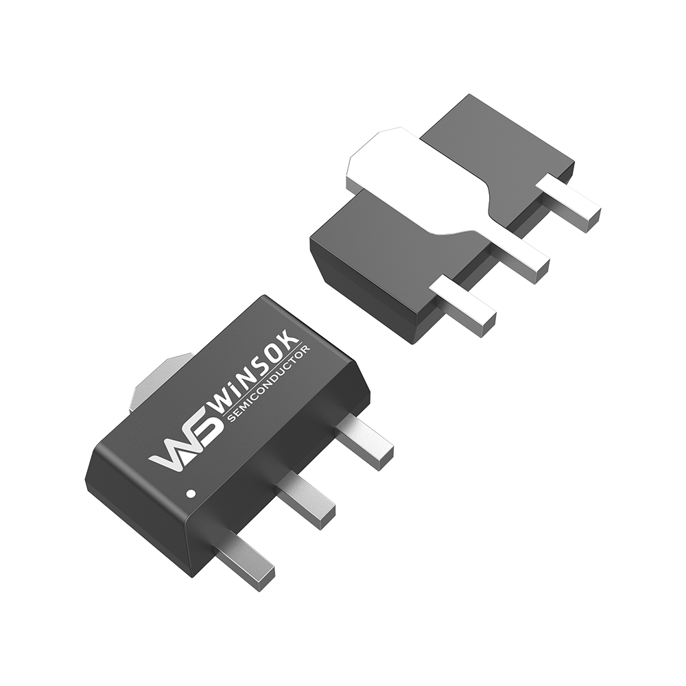
- Small power: SOT-23, SOT-223
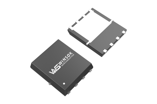
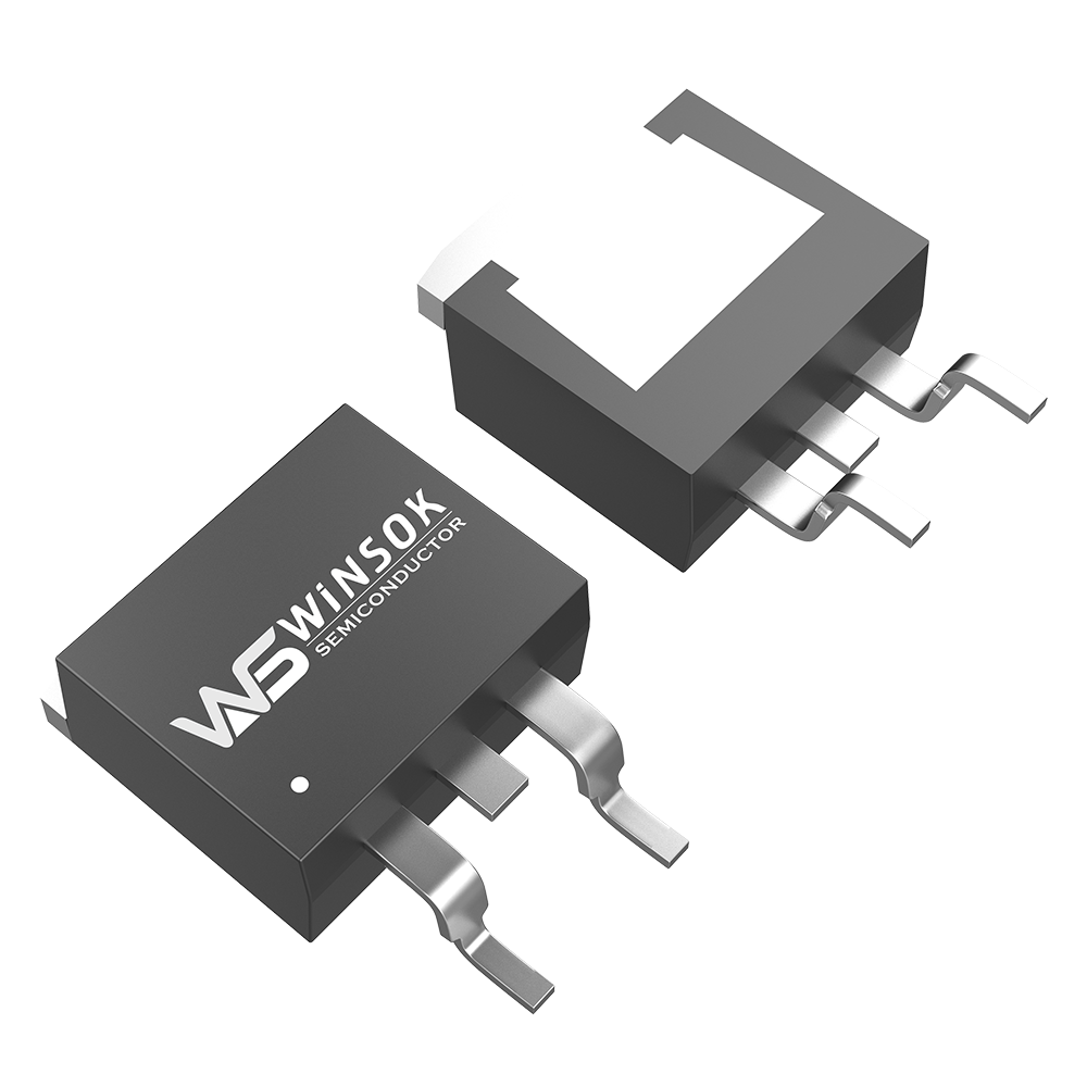
- Medium power: TO-220, TO-252
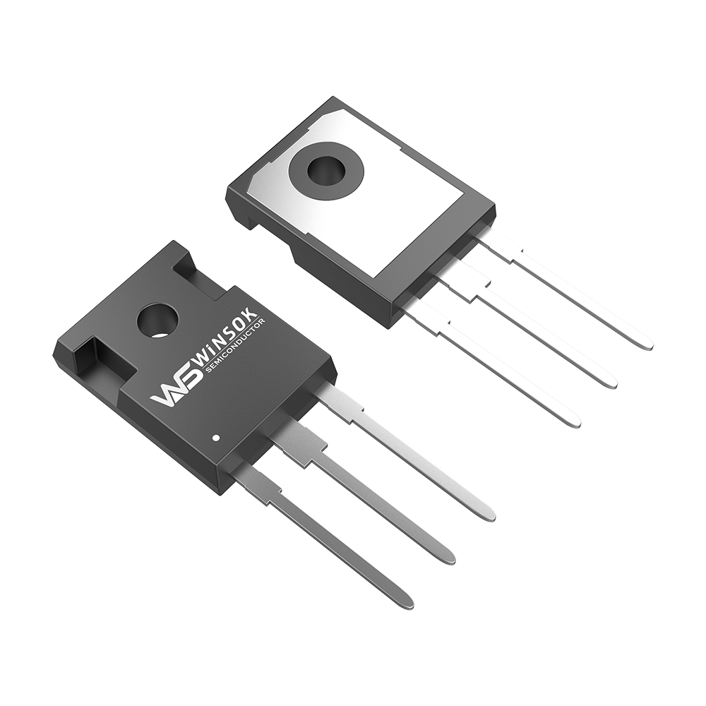
- High power: TO-247, SOT-227
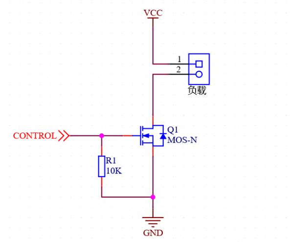
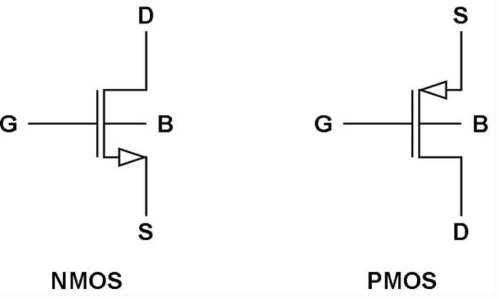
- N-channel: Widely used for low-side switching
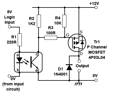
- P-channel: Applied to high-side power control
- 5-step Selection Guide
- 1.Confirm VDSS with sufficient voltage margin
- 2.Determine ID according to actual load current
- 3.Select low RDS(on) to minimize heating
- 4.Match driving voltage with threshold voltage
- 5.Verify gate charge, package and heat dissipation


-

Do You Know About MOSFET Circuits?
-

About MOSFET package type
-

Mastering Darlington Transistors: From Basic As...
-

Which brand of MOSFET is good
-

Understanding The Structure of Power MOSFET
-

Fast Switching MOSFET Circuits: Revolutionary P...
-
MOSFET Selection Points
-

How to Read & Describe MOSFET Specificatio...
-

Testing MOSFETs with a Multimeter: Essential St...
-

MOSFET Operating Characteristics
-

Unleashing the Power of MOSFETs and Transistors...
-

Fast Switching MOSFETs: The Complete Guide to N...
-
Understand MOSFET in onearticle
-
The right way to select MOSFETs
-
Main parameters of MOSFETs and comparison with ...
-

How much do you know about MOSFET parameters? O...


