


1. Introduction
Excessive temperature is the main cause of early‑failure for surface‑mount MOSFETs used in BLDC motor drivers and DC‑DC power circuits. SMD packages such as DPAK, IPAK, SO‑8 have limited chip‑to‑ambient heat dissipation area. Proper thermal‑design can reduce junction temperature, lower RDS(on) drift and extend service life. This article summarizes practical and mass‑production‑proven cooling solutions.
2. PCB Layout Optimization (Most Cost‑Effective Method)
2.1 Expand copper area under drain pad
The metal tab of SMD‑MOSFET connects to the drain internally. Lay large‑size copper foil directly underneath the MOSFET drain pad.
- Recommended copper area: At least 3 cm² for DPAK devices.
- Use 2‑oz copper thickness rather than standard 1‑oz copper for high‑current applications.
- Do not route signal traces over this copper region, keep the whole area intact for heat spreading.
2.2 Apply thermal vias
Drill multiple thermal vias through the drain copper pad to transfer heat to the bottom‑layer copper.
- Via size: 0.3‑0.4 mm diameter with 1.0‑1.2 mm pitch.
- Fill vias with copper plating; 6‑12 vias for DPAK‑type MOSFET is common.
- Bottom‑layer copper area should match the top‑layer copper size.
2.3 Reasonable component placement
- Separate multiple power MOSFETs; avoid putting them side‑by‑side otherwise heat will stack up mutually.
- Keep inductors and diodes away from MOSFETs to prevent extra heat interference.

3. Apply Thermal Interface Materials
3.1 Thermal paste and thermal pad
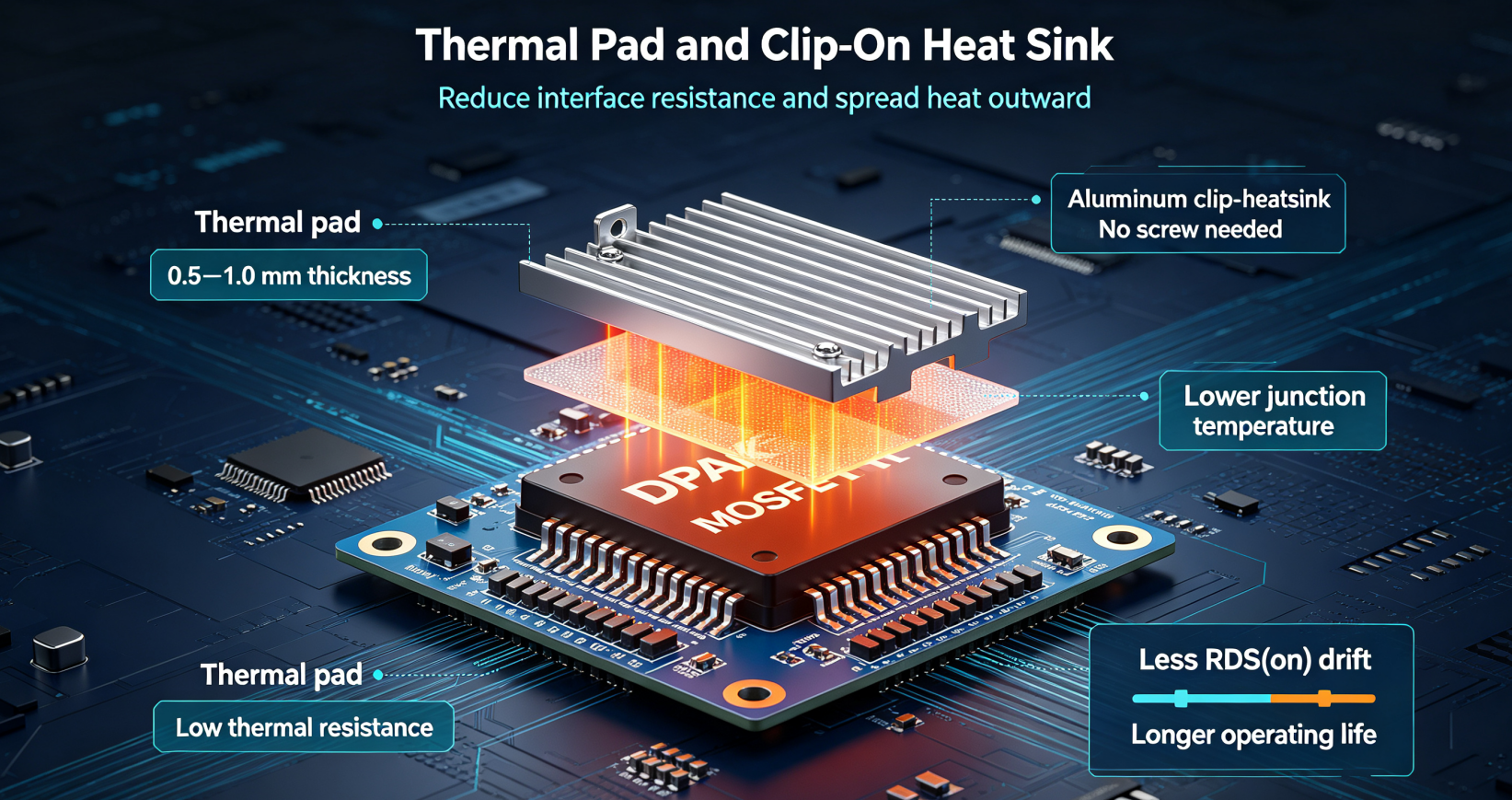
When you stick an external heat sink onto SMD‑MOSFET:
- Use soft silicone thermal pads of 0.5 mm‑1.0 mm thickness. Thermal resistance should be less than 1.5 W/m‑K.
- Avoid overly‑thick pads which increase thermal resistance.
3.2 SMD‑clip‑on heat sinks
Small clip‑on aluminum heat sinks are specially designed for DPAK and SO‑8 packages. They attach tightly to the MOSFET top surface without screws, suitable for mass‑production assembly.
4. Package‑Level Selection and Derating Design
4.1 Choose larger footprint if PCB space permits
IPAK package has a bigger metal tab compared with DPAK‑3, which brings lower RthJC value. If your board layout allows, upgrade from SO‑8 to DPAK‑3 for better heat‑dissipation performance.
4.2 Derate working current properly
RDS(on) rises as junction temperature increases. Do not run MOSFET at its maximum rated ID continuously.
- Keep actual continuous current within 70‑80% of datasheet ID rating for long‑term operation.
- Our Winsok DPAK MOSFETs are tested at 175 °C maximum junction temperature with tight‑tolerance parameters for BLDC‑motor projects.
5. System‑Level Cooling Methods
- Add forced‑air cooling with small fans for high‑power BLDC controllers.
- Enclosure design: Reserve ventilation holes to release internal hot‑air.
- Reduce switching‑loss by matched gate‑drive voltage and proper gate‑resistor. Less power loss fundamentally lowers heat generation.
6. Conclusion
The priority order to improve SMD‑MOSFET cooling:
- Optimize PCB copper area and thermal vias (first choice);
- Install clip‑on heat sinks or thermal pads;
- Select a larger MOSFET package and derate operating current;
- Optimize overall circuit to reduce power‑loss.
If these measures are well‑implemented, the junction temperature can drop by 20‑35°C effectively for BLDC‑H‑bridge circuits.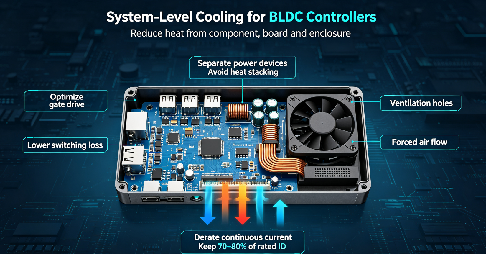


-

Circuit situation of mosfet application
-
What is MOSFET?
-

How much do you know about the MOSFET model cro...
-

MOSFET Failure Analysis: Understanding, Prevent...
-

CMS8H1213 MCU Cmsemicon® Package SSOP24 Batch 24+
-

MOSFET vs FET: Why Modern Electronics Choose Me...
-

Analysis of important causes of MOSFET heat gen...
-

RDS(on) in MOSFETs: The Critical Parameter for ...
-

MOSFET substitution principle and good and bad ...
-

What Are the Functions of MOSFETs in Lithium‑io...
-

How much do you know about MOSFET parameters? O...
-

Working with MOSFETs: Essential Knowledge for E...
-

Power MOSFET V-I Characteristics: Analysis and ...
-

Power MOSFET Construction: Advanced Technology ...
-

MOSFET 101: The Ultimate Beginner’s Guide...
-

Causes and Prevention of MOSFET Failure


