
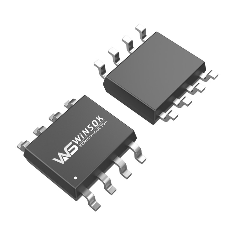
WSP4088 N-channel 40V 11A SOP-8 WINSOK MOSFET
General Description
The WSP4088 is the highest performance trench N-channel MOSFET with very high cell density providing excellent RDSON and gate charge for most synchronous buck converter applications. WSP4088 complies with RoHS and green product requirements, 100% EAS guarantee, full function reliability approved.
Features
Reliable and Rugged,Lead Free and Green Devices Available
Applications
Power Management in Desktop Computer or DC/DC Converters,Electronic cigarettes, wireless charging, motors, drones, medical, car charging, controllers, digital products, small household appliances, consumer electronics, etc
corresponding material number
AO AO4884 AO4882,ON FDS4672A,PANJIT PJL9424,DINTEK DTM4916 etc.
Important parameters
Absolute Maximum Ratings (TA = 25 C Unless Otherwise Noted)
| Symbol | Parameter | Rating | Unit | |
| Common Ratings | ||||
| VDSS | Drain-Source Voltage | 40 | V | |
| VGSS | Gate-Source Voltage | ±20 | ||
| TJ | Maximum Junction Temperature | 150 | °C | |
| TSTG | Storage Temperature Range | -55 to 150 | ||
| IS | Diode Continuous Forward Current | TA=25°C | 2 | A |
| ID | Continuous Drain Current | TA=25°C | 11 | A |
| TA=70°C | 8.4 | |||
| IDM a | Pulsed Drain Current | TA=25°C | 30 | |
| PD | Maximum Power Dissipation | TA=25°C | 2.08 | W |
| TA=70°C | 1.3 | |||
| RqJA | Thermal Resistance-Junction to Ambient | t £ 10s | 30 | °C/W |
| Steady State | 60 | |||
| RqJL | Thermal Resistance-Junction to Lead | Steady State | 20 | |
| IAS b | Avalanche Current, Single pulse | L=0.1mH | 23 | A |
| EAS b | Avalanche Energy, Single pulse | L=0.1mH | 26 | mJ |
Note a: Max. current is limited by bonding wire.
Note b: UIS tested and pulse width limited by maximum junction temperature 150oC (initial temperature Tj=25oC).
Electrical Characteristics (TA = 25 C Unless Otherwise Noted)
| Symbol | Parameter | Test Conditions | Min. | Typ. | Max. | Unit | |
| Static Characteristics | |||||||
| BVDSS | Drain-Source Breakdown Voltage | VGS=0V, IDS=250mA | 40 | - | - | V | |
| IDSS | Zero Gate Voltage Drain Current | VDS=32V, VGS=0V | - | - | 1 | mA | |
| TJ=85°C | - | - | 30 | ||||
| VGS(th) | Gate Threshold Voltage | VDS=VGS, IDS=250mA | 1.5 | 1.8 | 2.5 | V | |
| IGSS | Gate Leakage Current | VGS=±20V, VDS=0V | - | - | ±100 | nA | |
| RDS(ON) c | Drain-Source On-state Resistance | VGS=10V, IDS=7A | - | 10.5 | 13 | mW | |
| TJ=125°C | - | 15.75 | - | ||||
| VGS=4.5V, IDS=5A | - | 12 | 16 | ||||
| Gfs | Forward Transconductance | VDS=5V, IDS=15A | - | 31 | - | S | |
| Diode Characteristics | |||||||
| VSD c | Diode Forward Voltage | ISD=10A, VGS=0V | - | 0.9 | 1.1 | V | |
| trr | Reverse Recovery Time | VDD=20V,ISD=10A, dlSD/dt=100A/ms | - | 15.2 | - | ns | |
| ta | Charge Time | - | 9.4 | - | |||
| tb | Discharge Time | - | 5.8 | - | |||
| Qrr | Reverse Recovery Charge | - | 9.5 | - | nC | ||
| Dynamic Characteristics d | |||||||
| RG | Gate Resistance | VGS=0V,VDS=0V,F=1MHz | 0.7 | 1.1 | 1.8 | W | |
| Ciss | Input Capacitance | VGS=0V,VDS=20V,Frequency=1.0MHz | - | 1125 | - | pF | |
| Coss | Output Capacitance | - | 132 | - | |||
| Crss | Reverse Transfer Capacitance | - | 70 | - | |||
| td(ON) | Turn-on Delay Time | VDD=20V, RL=20W,IDS=1A, VGEN=10V, RG=1W | - | 12.6 | - | ns | |
| tr | Turn-on Rise Time | - | 10 | - | |||
| td(OFF) | Turn-off Delay Time | - | 23.6 | - | |||
| tf | Turn-off Fall Time | - | 6 | - | |||
| Gate Charge Characteristics d | |||||||
| Qg | Total Gate Charge | VDS=20V, VGS=4.5V, IDS=7A | - | 9.4 | - | nC | |
| Qg | Total Gate Charge | VDS=20V, VGS=10V, IDS=7A | - | 20 | 28 | ||
| Qgth | Threshold Gate Charge | - | 2 | - | |||
| Qgs | Gate-Source Charge | - | 3.9 | - | |||
| Qgd | Gate-Drain Charge | - | 3 | - | |||
Note c:
Pulse test ; pulse width£300ms, duty cycle£2%.
Why Choose Us?
Better Than Factory Prices
Competitive pricing that beats direct factory offers through our strategic partnerships
Fast Shipping
Large inventory ready for immediate dispatch with quick delivery times
Premium Service
Superior customer support and technical assistance throughout your journey
FAQ
How to Place an Order?
1. Submit inquiry through our website
2. Receive quotation within 24 hours
3. Confirm order details and make payment
4. Order processing and shipping
MOQ & Payment Terms
• Standard MOQ: 1000 pieces
• Sample order: 10-50 pieces
• Payment Terms: 30% deposit, 70% before shipment
Payment Methods
• T/T (Bank Transfer)
• Letter of Credit (L/C)
• Western Union
• PayPal (for sample orders)
Shipping & Delivery
• Warehouses: Hong Kong & Shenzhen
• Delivery time: 3-5 days after payment
• Express services: DHL, FedEx, UPS
• Air freight available for bulk orders
Certifications & Quality Assurance

ISO 9001:2015
Quality Management System Certified

RoHS Compliant
Environmental Protection Standard

REACH Compliant
European Union Safety Standard
Customer Testimonials
Real feedback from our global customers, witnessing our quality and service excellence

Olukey's MOSFETs consistently deliver stable quality with precise delivery times. We've made multiple purchases and remain highly satisfied.
Procurement Manager @ XYZ Electronics (India)

Competitive pricing coupled with responsive technical support helped us optimize our circuit design effectively.
Supply Chain Executive @ TechPower Solutions (Vietnam)

From small batch testing to mass production, our cooperation has been seamless. A truly reliable long-term partner.
Hardware Engineer @ BrightCircuit Innovations (Malaysia)
Our Trusted Partners
Our products are successfully implemented in smart devices, power adapters, and industrial equipment by global brands


📌Choose Olukey for a More Efficient and Reliable Supply Chain!
-

STL52DN4LF7AG STL64DN4F7AG PJQ5442 PDC496X N-ch...
-
WSD6040DN56 N-channel 60V 36A DFN5X6-8 WINSOK M...
-

WST3428 N-channel 20V 2.3A SOT-23-3L WINSOK MOSFET
-

WSR150N15 N-channel 150V 150A TO-220-3L WINSOK ...
-

WSD27N10DN56 N+P-channel ±100V 18A/-12A DFN5X6-...
-
WSR80N08 N-channel 80V 80A TO-220-3L WINSOK MOSFET


