
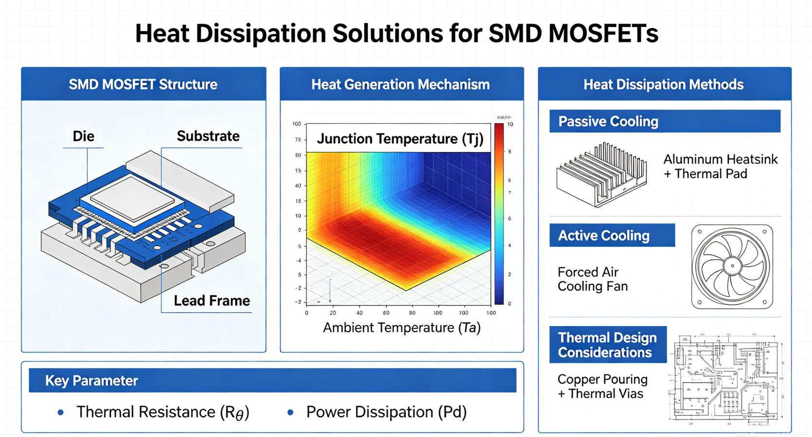
Heat Dissipation Solutions for SMD MOSFETs
Effective thermal management is essential for ensuring the reliability, efficiency, and longevity of SMD (Surface-Mount Device) MOSFETs. In high-current and high-frequency applications such as power supplies, inverters, motor drives, and battery management systems, proper heat dissipation is critical.
1. Increase PCB Copper Area (Most Common Method)
The heat generated by a MOSFET is primarily transferred to the PCB through its leads and exposed thermal pad. Expanding the copper area connected to the Drain terminal is one of the most cost-effective cooling solutions.
Design Recommendations:
- Maximize the copper area connected to the Drain.
- Use copper pours on both top and bottom PCB layers.
Recommended copper thickness:
- 1 oz (35 μm) for standard applications.
- 2 oz or 3 oz for high-current applications.
Typical Thermal Improvement:
Copper Area Temperature Reduction
- 1 cm² Approximately 10–15°C
- 4 cm² Approximately 20–30°C
2. Add Thermal Vias
For packages such as DFN, PDFN, PowerPAK, and TO-263, thermal vias should be placed beneath the exposed thermal pad.
Recommended Parameters:
- Via diameter: 0.2–0.3 mm
- Via pitch: 0.8–1.2 mm
- Quantity: 9–25 vias or more
Advantages:
✔ Rapidly transfers heat to inner and bottom PCB layers.
✔ Can reduce junction temperature by 10–20°C.
Design Notes:
- Filled or plugged vias (Via-in-Pad Filled) are recommended.
- Prevent solder wicking during the assembly process.
3. Double-Sided Copper Spreading
Heat can be transferred from the top copper layer to the bottom layer through thermal vias, significantly improving heat dissipation.
MOSFET
↓
Top Copper Layer
↓
Thermal Vias
↓
Bottom Copper Layer
Typical Applications:
DC-DC converters
Battery protection circuits
Drone ESCs
Fast-charging systems
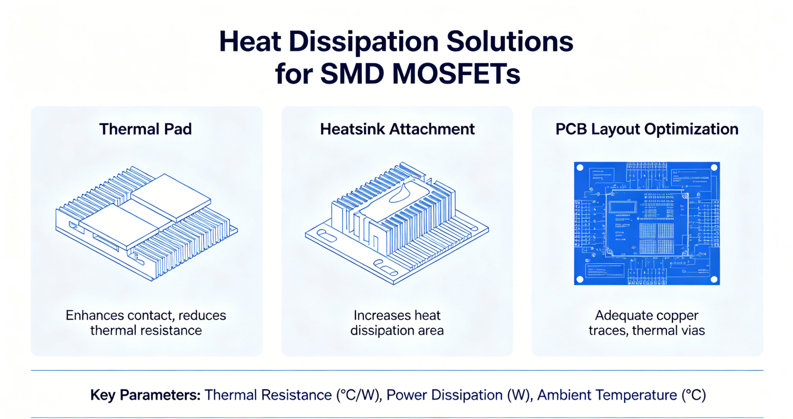
4. Attach a Heat Sink (For High-Power Applications)
When MOSFET power dissipation exceeds 3 W to 5 W, PCB copper alone may not provide sufficient cooling.
Optional Cooling Solutions:
- Aluminum heat sinks
- Copper heat sinks
- Clip-on heat sinks
- Thermal pads combined with metal chassis cooling
Common Applications:
- Inverters
- Power tools
- Energy storage systems
- Motor drive systems
5. Use Metal Core PCB (MCPCB)
For high-power applications, a Metal Core PCB (MCPCB) can significantly enhance thermal performance.
Typical Structure:
- Copper Layer
- Insulation Layer
- Aluminum Base
Features:
- Thermal conductivity is typically 3 to 8 times higher than conventional FR4 PCBs.
- Widely used in LED drivers, power modules, and automotive electronics.
6. Forced Air Cooling
If system space allows, additional cooling can be achieved by:
- Cooling fans
- Optimized airflow channels
- Blowers
Forced air cooling can typically reduce MOSFET temperature rise by 20% to 50%.
Recommended Cooling Methods by Power Dissipation
MOSFET Power Dissipation Recommended Cooling Method
- < 1 W Large copper area only
- 1 W – 3 W Copper area + thermal vias
- 3 W – 5 W Double-sided copper + thermal vias
- 5 W – 10 W Heat sink or forced air cooling
- > 10 W Heat sink + forced air cooling or MCPCB
PCB Layout Considerations
✅ Place MOSFETs near the PCB edge to improve airflow.
✅ Ensure uniform heat distribution when multiple MOSFETs are connected in parallel.
✅ Keep MOSFETs away from other heat-generating components such as inductors and diodes.
✅ Keep high-current paths short and wide to minimize conduction losses.
✅ Use wide traces or solid copper planes for high-current applications.
For WINSOK SMD MOSFET packages such as DFN5×6, PDFN3.3×3.3, and TO-252, the combination of large copper areas, thermal vias, and double-sided copper planes is recommended for most power supply and inverter applications.


-

Heat Dissipation Solutions for SMD MOSFETs
-

What is the difference between MOSFET and IGBT?...
-
What are the differences between MOSFETs and Tr...
-

What Is a Switched Mode Power Supply?
-

Power MOSFET Construction: Advanced Technology ...
-

MOSFET Classification Characteristics
-
Understand the working principle of MOSFET and ...
-

Power MOSFET V-I Characteristics: Analysis and ...
-
What parameters should I pay attention to when ...
-

How to Use a MOSFET: Complete Guide for Beginne...
-

The importance of power MOSFET in motherboard d...
-
How can I tell the difference between a Mosfets...
-

How to prevent MOSFET failure
-

How to Measure MOSFET Power Breakdown: A Compre...
-
MOSFET Package Switching Tube Selection and Cir...
-

Understanding MOSFET Overdrive Voltage: Compreh...


