


1. Preface
MOSFET selection directly affects circuit efficiency, heat generation, service life and stability. Many engineers only focus on voltage and current ratings while ignoring key performance indicators, which easily leads to excessive loss, overheating or device breakdown. This article sorts out a complete step-by-step evaluation standard for MOSFET parameters for power supply, BLDC motor, battery management and switching circuit design.
2. Step 1: Evaluate Absolute Maximum Voltage Parameters
2.1 VDS (Drain-Source Rated Voltage)
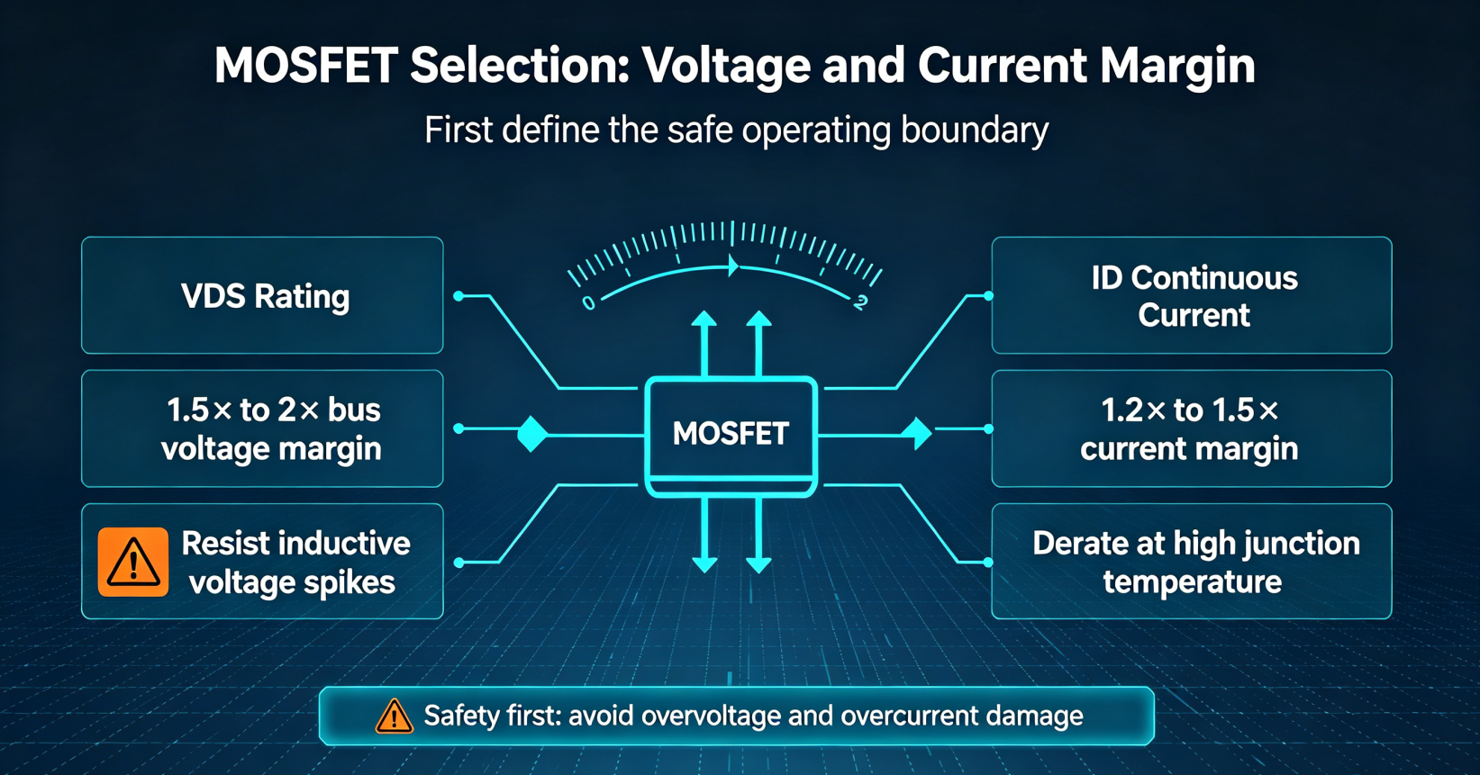
Select a VDS margin of at least 1.5~2 times the actual circuit bus voltage.
- For low-voltage DC circuits below 48V: leave 1.5x voltage margin
- For high-frequency switching power supplies, inverter circuits: leave 2x margin to resist voltage spikes induced by inductance
If VDS margin is insufficient, the MOSFET will suffer avalanche breakdown during switching transient spikes.
2.2 VGS (Gate-Source Rated Voltage)
Most silicon MOSFETs support ±20V gate-source voltage.
- 3.3V/5V small-signal drive circuits: confirm the threshold voltage matches the driving level
- High-voltage gate drive circuits: add gate clamping circuit to avoid exceeding the VGS limit and burning the gate oxide layer
2.3 VGS(th) Threshold Voltage (Enhancement MOS)
- Low VGS(th) devices: suitable for low-voltage MCU direct drive
- High VGS(th) devices: stronger anti-interference, less prone to false turn-on under noise
Match the threshold voltage with the actual driving voltage amplitude of the circuit.
3. Step 2: Evaluate Current Load Capacity
3.1 ID Continuous Drain Current
The rated ID under specified shell temperature must be higher than the actual maximum operating current of the circuit, with a 1.2~1.5 times margin reserved.
Note that ID will drop significantly when the junction temperature rises, so high-current continuous working scenarios cannot rely solely on the room-temperature ID parameter.
3.2 IDM Pulse Drain Current
Evaluate according to peak instantaneous current such as startup current, inrush current and short-circuit current.
If the circuit has large pulse current impact, prioritize devices with high IDM specifications.
3.3 ISD Body Diode Current
For synchronous rectification, H-bridge BLDC drive circuits, the internal body diode will bear reverse freewheeling current. Check whether ISD meets the freewheeling current requirement.
4. Step 3: Evaluate Conduction Loss Core Index – RDS(on)
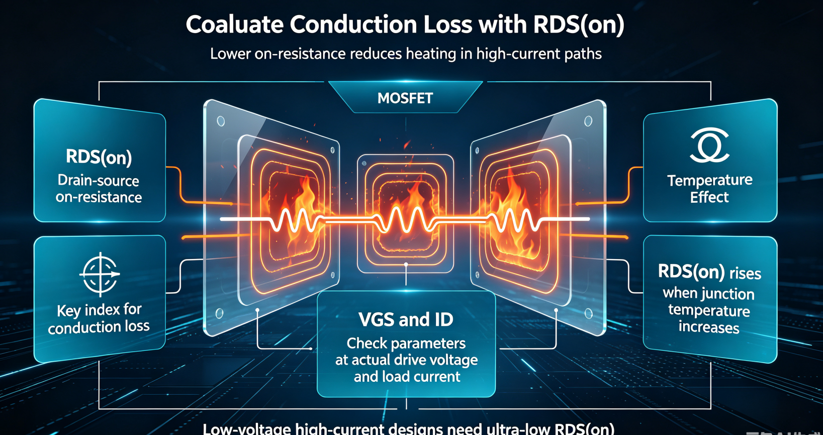
RDS(on) is the core parameter that determines conduction heating, and it must be evaluated under actual VGS, ID and junction temperature conditions.
- Low-voltage large-current scenarios (battery equipment, vehicle load): prioritize ultra-low RDS(on) MOSFETs to reduce conduction loss
- High-frequency small-current circuits: do not blindly pursue ultra-low RDS(on), balance gate charge cost
- Note: RDS(on) will rise with temperature; calculate heat generation based on the RDS(on) value at maximum TJ
5. Step 4: Evaluate Switching Performance for High-Frequency Circuits
5.1 Gate Charge Qg, Qgd Miller Charge
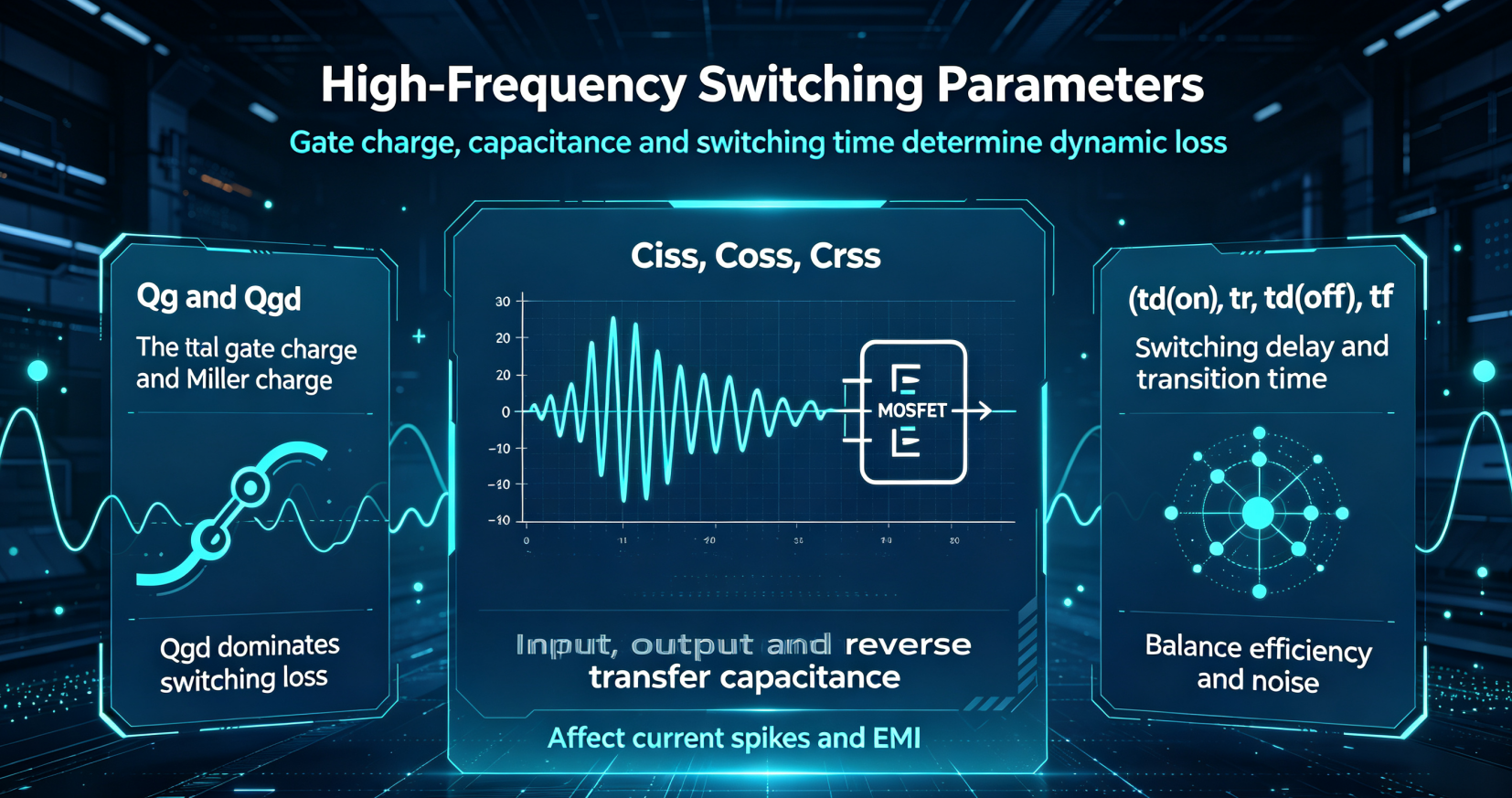
Qg determines the driving power consumption of the peripheral driver chip; Qgd is the main source of switching loss.
- High-frequency SMPS above 100kHz: select low Qgd devices to reduce switching heat
- Low-frequency motor drive below 20kHz: Qg has little influence, priority to low RDS(on)
5.2 Parasitic Capacitance Ciss, Coss, Crss
Large parasitic capacitance will cause large current spikes during switching and increase EMI interference. High-frequency design needs to choose MOSFET with small parasitic capacitance.
5.3 Switching Time td(on), tr, td(off), tf
Shorter switching time reduces switching loss, but will increase electromagnetic interference; select a balance point according to EMC requirements of the product.
6. Step 5: Evaluate Body Diode Recovery Characteristics
6.1 trr Reverse Recovery Time
For synchronous rectifier, inverter and bridge drive circuits, trr directly affects reverse recovery loss.
- Fast recovery MOSFET (small trr): suitable for high-frequency synchronous rectification
- Slow recovery devices: easy to generate large reverse current spikes, increase loss and noise
6.2 VSD Diode Forward Voltage
Lower VSD reduces freewheeling loss of the body diode during dead time.
7. Step 6: Evaluate Thermal Parameters
7.1 TJ Maximum Junction Temperature
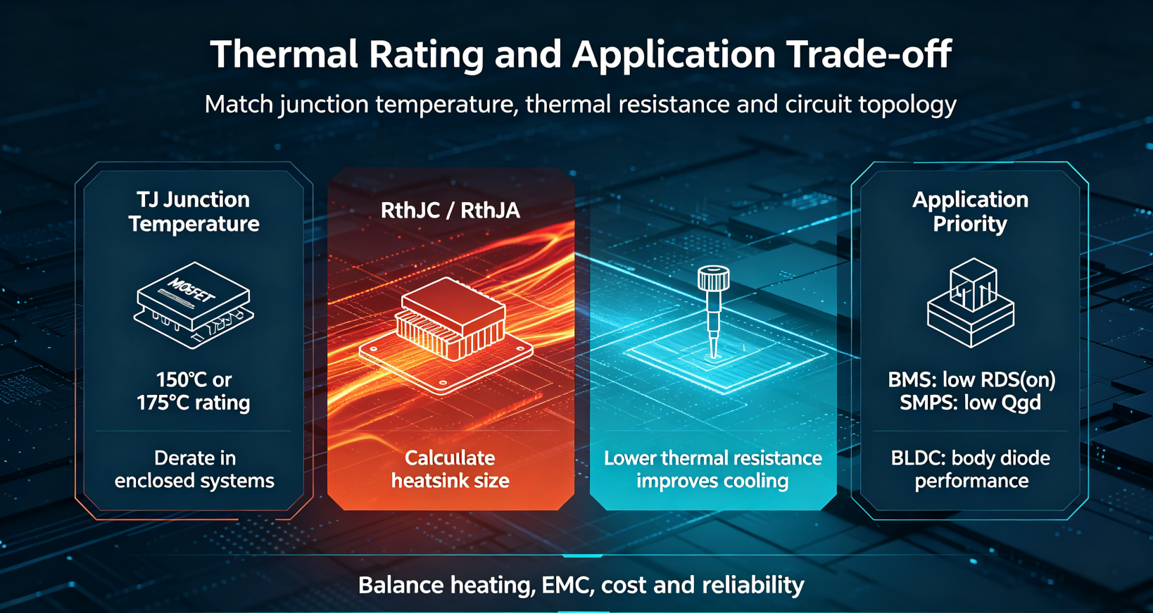
Conventional silicon MOSFET maximum junction temperature is 150°C or 175°C. Closed equipment with poor heat dissipation needs to select devices supporting 175°C TJ.
7.2 Thermal Resistance RthJC / RthJA
RthJC represents the heat conduction capacity from chip to shell; low thermal resistance matches small heat sinks. Calculate the required heat sink size by combining power loss and thermal resistance.
8. Step 7: Scene-Oriented Comprehensive Trade-off Principles
8.1 Low-Voltage High-Current Applications (BMS, DC-DC step-down)
Primary priority: Low RDS(on), sufficient ID current margin
Secondary consideration: Gate charge, cost
8.2 High-Frequency Switching Power Supply
Primary priority: Low Qgd, small parasitic capacitance, fast switching speed
Secondary consideration: Appropriately low RDS(on)
8.3 BLDC Motor H-Bridge Drive
Primary priority: Sufficient ID, good body diode freewheeling performance, moderate switching speed to suppress EMI
Secondary consideration: Thermal resistance
8.4 Low-Signal Low-Frequency Control
Primary priority: Matching VGS(th) with driving voltage, low gate leakage current
Secondary consideration: Cost
9. Summary of Parameter Evaluation Logic
- First lock safety boundaries: VDS voltage margin, ID current margin, maximum junction temperature to avoid device damage
- Second calculate power loss: judge conduction loss by RDS(on), judge switching loss by gate charge and parasitic capacitance
- Third match circuit frequency and topology: evaluate diode recovery characteristics for bridge and synchronous rectifier circuits
- Finally comprehensive trade-off: balance heat generation, EMC performance, device cost according to product application scenarios


-

How to Choose a MOSFET: The Complete Selection ...
-

What is the difference between MOSFET and IGBT?...
-

MOSFET type and construction
-
Understand MOSFET in onearticle
-

How much do you know about the MOSFET model cro...
-

MOSFET Selection Guide —-A PRACTICAL HAND...
-

Lithium battery charging is easy to damage, WIN...
-

Do you know what an N-channel MOSFET is?
-

Best Places to Source Quality MOSFET Transistor...
-

Advantages of Silicon Carbide (SiC) Power Devices
-
How to choose MOSFET?
-

Determining MOSFET Threshold Voltage: Expert Te...
-

Important Steps on MOSFET Selection
-

Operating Frequency Range of SiC MOSFET
-

Ultimate Guide to MOSFET Power Amplifiers: Unde...
-

Do you know the MOSFET driver circuit?


