


The MOSFET market is evolving along four main paths: silicon structural upgrading, wide-bandgap (WBG) material substitution, packaging/integration intelligence, and AI-assisted design, with high voltage, high frequency, high efficiency and low cost as the core competition dimensions.
In this process, Winsok Semiconductor — leveraging decades of R&D experience in power semiconductors — has become a key player in medium- and low-voltage MOSFETs and power management solutions, actively driving technology implementation and domestic substitution.
1. Silicon-Based MOSFETs: Structural Shrinkage and Performance Limits
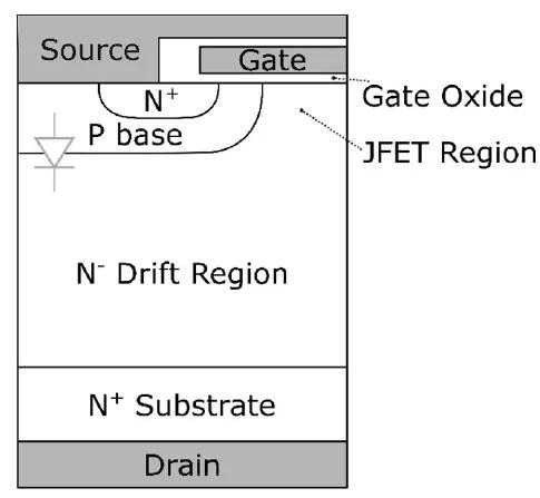
In the low-voltage market (below 200 V), silicon remains dominant, continuing its vitality through structural innovation. Winsok Semiconductor has a strong footprint in this segment, with products covering the 0–1200 V voltage range, especially in mass production of trench and shielded-gate (SGT) MOSFETs for medium and low voltages.
Super Junction (SJ) – A milestone for high-voltage MOSFETs. The vertical P-pillar structure reduces Rds(on)×Area for 600 V class devices to below 0.4 Ω·mm², cutting on-resistance by over 60% while maintaining lower switching losses than IGBTs.
Trench / Micro-Trench – Cell density doubles, continuously reducing Rds(on). With 12-inch wafer adoption, die cost drops by ~30%. Winsok specializes in trench technology, offering a wide range of ultra-small packages such as DFN2×2, DFN3×3 for fast chargers and portable devices.
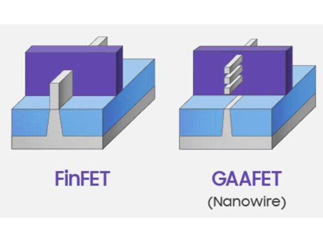
FinFET → GAA → CFET – Advanced logic/power ICs migrate from FinFET to GAA (Gate-All-Around), reducing leakage by over 50%. Below 3 nm (2026), CFET (Complementary FET) will vertically stack n/p transistors for further area reduction and frequency increase.
2. Wide-Bandgap (SiC/GaN): High-Voltage & High-Frequency Main Battlefield
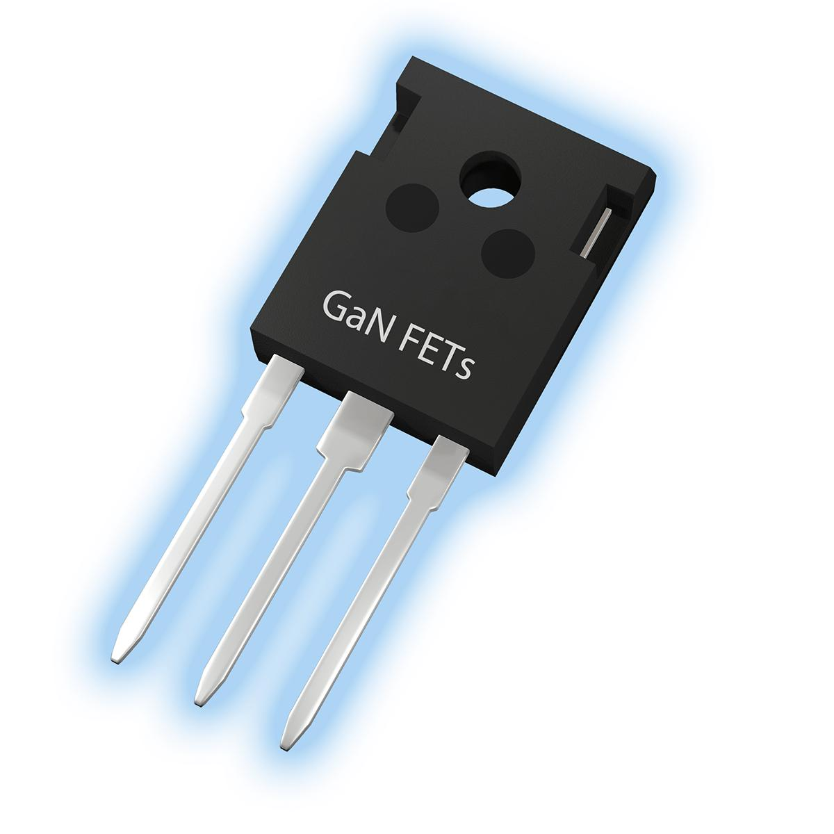
SiC targets high voltage (≥600 V), GaN targets high frequency (MHz range), rapidly replacing silicon in high-end applications. Winsok Semiconductor has launched R&D programs for both SiC and GaN devices, focusing on automotive OBC, industrial power supplies, and data center power delivery.
2.1 SiC MOSFETs (Silicon Carbide)
Key advantages – Breakdown field 3× higher than silicon, high temperature resistance (>200 °C), low conduction and switching losses. In 800 V EV traction systems, efficiency improves by 5–10%, increasing cold-range mileage by ~45 km.
Technology roadmap – 4th-gen SiC MOSFETs (2026) achieve mass production of 1200 V / 13 mΩ automotive-grade devices; 1700 V devices are mature. Domestic 8/12-inch fabs expand capacity, lowering costs by 30–40% vs. imports.
2.2 GaN MOSFETs (Gallium Nitride)
Key advantages – High electron mobility, switching frequency up to 10 MHz, ideal for fast chargers, 48 V AI server power, and automotive OBC.
Market explosion – Fast charger penetration accelerates in 2026; 11 kW OBC enables 280 km range recovery in 10 minutes. Data center server power density increases 3–5×, driving strong GaN demand. Winsok’s accumulated high-frequency MOS design experience provides a solid foundation for future GaN productization.
3. Packaging & Integration: Higher Power Density, Lower Parasitics
Advanced packaging – QDPAK / TOLL replaces traditional TO-220, reducing thermal resistance by ~40%. Silver sintering replaces solder for higher temperature resistance and 3× higher thermal conductivity. 2D/3D packaging (e.g., embedded die) minimizes parasitic inductance, improving switching performance by over 15%. Winsok offers volume production in TOLL, SOP-8, DFN and other packages, balancing thermal performance and miniaturization.
Smart MOSFETs – Integrate temperature sensors, current mirrors, and protection circuits, providing on-chip over-current/over-temperature protection and reducing system-level sensor latency.
Driver-in-MOSFET – Co-packaging of driver IC and MOSFET simplifies PCB design, reduces parasitics, and significantly improves high-frequency stability. Winsok has released multiple power device solutions with integrated drivers and protection for motor drive and fast charging applications.
4. AI & Design Methodology: Faster Iteration, Optimized Performance
AI-assisted design – Machine learning (e.g., genetic algorithms) optimizes doping and channel parameters, reducing Rds(on) by ~20%. Neural networks predict failure modes to enhance reliability. TSMC uses AI to shorten 5 nm cycle time by ~30%. Winsok is gradually adopting AI simulation and parameter optimization tools to accelerate new product development.
TCAD + SPICE co-simulation – Precise device physics modeling shortens R&D cycles, with BSIM3v3 model error controlled within 5%.
5. Market Landscape & Key Trends (2026–2028)
Silicon – Dominant in cost-sensitive low/medium-voltage (≤200 V) applications, with ongoing SJ/trench optimization and rising 12-inch wafer share. Winsok expands its presence in consumer electronics, fast chargers, and industrial controls via a broad medium/low-voltage MOSFET portfolio and fast customization capability.
SiC – Strong growth in 800 V EVs, PV inverters, industrial power supplies; EV traction penetration exceeds 30% in 2026, accelerating domestic substitution.
GaN – Rapid expansion in fast chargers, AI data centers, OBC; silicon replacement accelerates in high-frequency applications below 200 V.
Integration & Intelligence – Smart MOSFETs and driver-in-MOSFET become standard in high-end power supplies, simplifying design and improving efficiency.
Conclusion
The MOSFET market is shifting from silicon-only evolution to silicon + WBG dual-track development: silicon defends low-voltage cost markets via structural upgrades, while SiC/GaN capture high-voltage/high-frequency territories through material advantages. Advanced packaging and AI design further boost performance and reliability. Winsok Semiconductor — building on mature silicon power devices and actively expanding into WBG and intelligent power integration — is strategically positioned in the global MOSFET technology revolution and domestic substitution wave.


-

How to distinguish between P-channel and N-chan...
-

How to Determine nMOSFETs and pMOSFETs
-

How to Test MOSFETs in Motor Controllers?
-

Small Signal Model MOSFET Analysis and Implemen...
-

Why the Absolute‑Value of PMOS Threshold‑Voltag...
-
The three main roles of MOSFETs
-

How Long Do MOSFETs Last? A Comprehensive Guide...
-

MOSFET Selection Guide —-A PRACTICAL HAND...
-

Briefly talk about the production method of a h...
-

Comprehensive Guide: Driving MOSFETs with Optoc...
-

Causes and Prevention of MOSFET Failure
-

Do you know the three poles of MOSFET?
-

Common Gate MOSFET Amplifier: A Comprehensive A...
-

Original spot CMS79F726 package SOP20 touch but...
-

How to Select Gate Resistor for Anti-Reverse MO...
-

How to Judge MOSFET Working State According to ...


