


1. Clarify a crucial concept
For enhancement‑mode power‑MOSFET:
- NMOS threshold voltage VGS(th) is positive, typical range:0.7V‑1.0V.
- PMOS threshold voltage VGS(th) is negative, normally ‑0.9V ~ ‑1.3V.
We compare absolute value here. PMOS does not have a bigger numerical reading, but a larger magnitude of threshold‑voltage. This difference greatly influences BLDC H‑bridge performance.

2. Three core causes
2.1 Carrier mobility difference (primary reason)
Current inside NMOS depends on electrons, whose mobility reaches about 1350 cm²/(V·s).
PMOS relies on holes for conduction. Hole mobility is only roughly 480 cm²/(V·s), about one‑third of electrons.
With identical channel dimension and gate‑oxide thickness, holes are much harder to move. Chip manufacturers must apply a higher‑magnitude gate‑source voltage to build a stable conducting channel. If PMOS uses the same threshold‑voltage level as NMOS, the channel will be weak and produce high on‑resistance.
2.2 Difference between substrate structures
- NMOS is built on a P‑type substrate.
- PMOS is fabricated within an N‑well which is implanted into the P‑substrate.
The N‑well creates inherent built‑in potential. Higher doping concentration widens depletion‑region. It requires larger gate bias voltage to form inversion‑layer, which increases the absolute threshold‑voltage for PMOS.
2.3 Gate‑material work‑function mismatch
Polysilicon gate has different work‑function on P‑well and N‑well. This material‑related deviation brings additional threshold‑voltage offset for PMOS. Even with identical SiO₂ thickness, PMOS still needs higher driving voltage.

3. Practical effects on BLDC‑motor projects
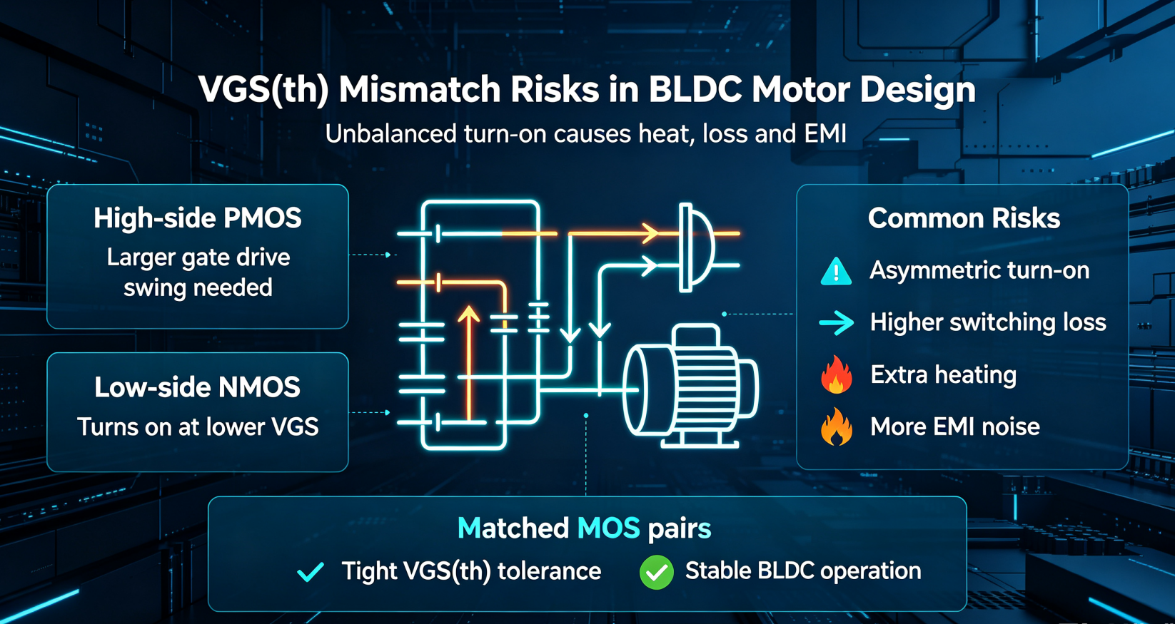
- PMOS needs sufficient gate‑drive voltage to turn‑on fully. Insufficient voltage pushes PMOS into saturation region and results in severe heat generation.
- Excessive VGS(th) gap between high‑side PMOS and low‑side NMOS causes asynchronous turn‑on, which raises switching loss and EMI noise.
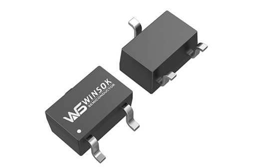
- Our Winsok PMOS keeps threshold‑voltage tolerance within ±0.15V. Well‑matched NMOS‑PMOS pairs cooperate with China‑Micro MCU to deliver stable performance for BLDC‑mass‑production.
4. Conclusion
Slow‑moving holes, N‑well substrate and gate‑material differences make PMOS have higher absolute threshold‑voltage than NMOS. Choosing matched MOS pairs is essential for high‑efficiency BLDC‑motor systems.


-

The Complete Guide to MOSFET Amplifiers: From B...
-

2N7002 LTspice Modeling and Simulation Guide
-
Understand the working principle of MOSFET and ...
-
MOSFET overview
-

MOSFET gate source protection
-

The connection between MOSFETs and Field Effect...
-

The three pins of a MOSFET, how can I tell them...
-
About the working principle of power MOSFET
-

Heat Dissipation Solutions for SMD MOSFETs
-

De rol van vermogens-MOSFET-apparaten
-

Why are N channel MOSFET preferred over P chann...
-

Building the Perfect Ideal Diode with MOSFETs: ...
-

A Comprehensive Guide about What is VGS in MOSFET
-

How to distinguish between P-channel and N-chan...
-
What is MOSFET?
-

Floating Gate MOSFET Implementation: Key Steps ...


