
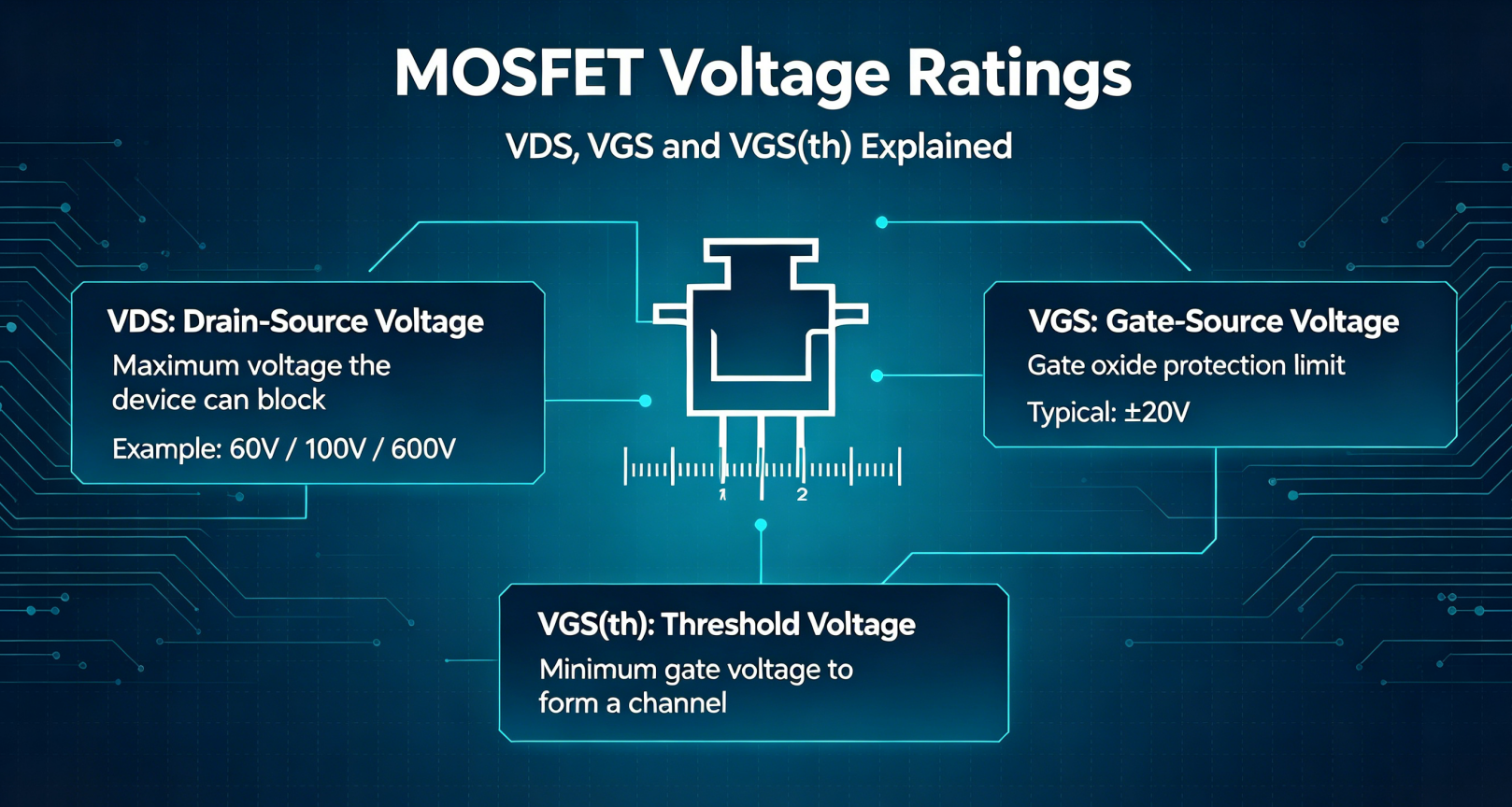
1. Core Voltage Ratings (Absolute Maximum Ratings)
1.1 VDS – Drain-Source Voltage
The maximum allowable voltage between drain and source under normal operation. Exceeding this value will cause avalanche breakdown and permanent damage to the MOSFET.
- Example marking: VDS = 60V, 100V, 200V, 600V
1.2 VGS – Gate-Source Voltage
Maximum safe voltage applied to gate and source. Gate oxide layer is extremely thin; overvoltage leads to gate punch-through.
- Standard range: ±20V for most silicon MOSFETs
1.3 VGS(th) / VGS(off)
- Enhancement MOS: VGS(th) = Threshold voltage, minimum VGS to form conductive channel
- Depletion MOS: VGS(off) = Pinch-off voltage, negative bias to cut off native channel
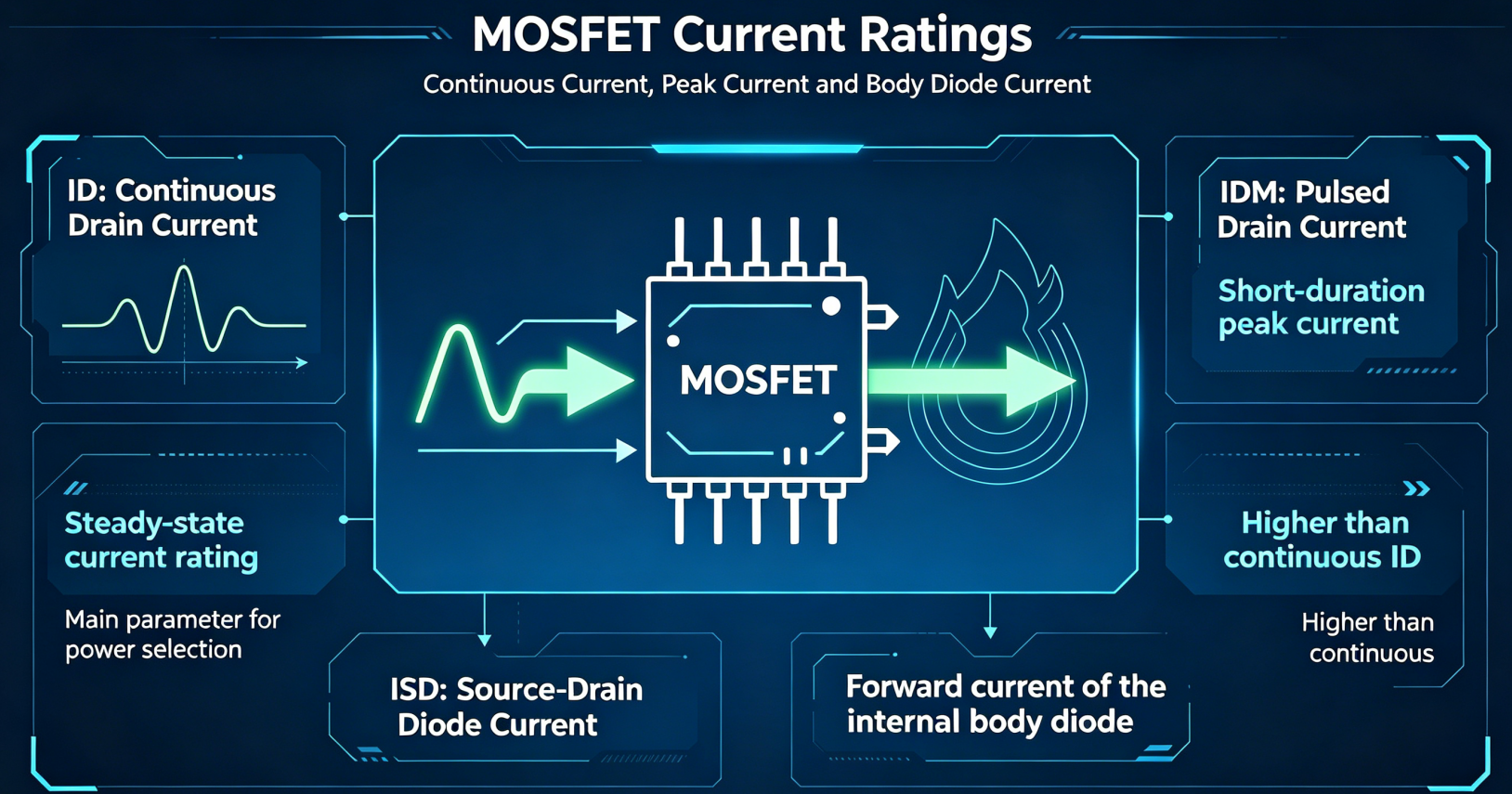
2. Current Parameters
2.1 ID – Continuous Drain Current
Maximum steady-state drain current the device can carry at specified case temperature, the main current rating for power applications.
2.2 IDM – Pulsed Drain Current
Peak transient current allowed for short pulse durations, much higher than continuous ID.
2.3 ISD – Source-Drain Diode Current
Forward current rating of the internal body diode inside MOSFET.
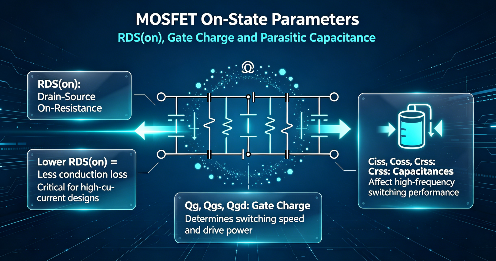
3. On-State Conduction Parameters
3.1 RDS(on) – Drain-Source On-Resistance
Key performance index: resistance between drain and source when MOS is fully turned on at specified VGS and ID.
Lower RDS(on) = less conduction loss, lower heat generation.
3.2 Qg, Qgs, Qgd – Gate Charge
Total gate charge required to switch the MOSFET on/off, determines switching speed and drive power consumption.
- Qgd (Miller charge) dominates switching loss in high-frequency circuits.
3.3 Ciss, Coss, Crss – Parasitic Capacitances
Input capacitance, output capacitance, reverse transfer capacitance; critical for high-frequency SMPS, BLDC inverter designs.
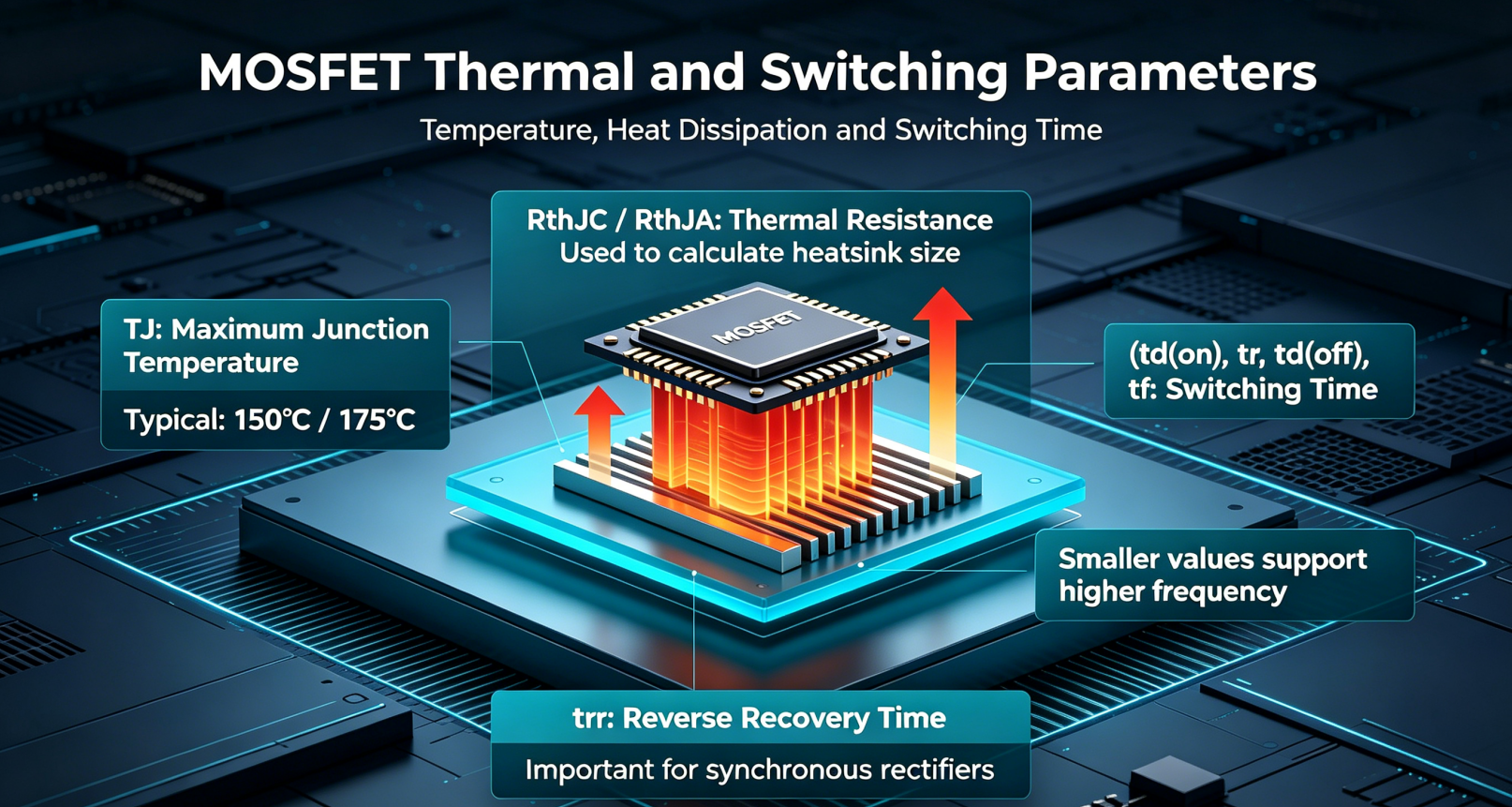
4. Switching Time Parameters
4.1 td(on), tr, td(off), tf
Turn-on delay time, rise time, turn-off delay time, fall time.
Smaller values support higher operating switching frequency.
5. Thermal & Derating Parameters
5.1 TJ – Maximum Junction Temperature
Max internal chip temperature, typical 150°C / 175°C.
5.2 RthJC / RthJA
Thermal resistance junction-to-case, junction-to-ambient; used to calculate required heat sink size.
6. Body Diode Parameters
6.1 VSD – Body Diode Forward Voltage
Forward voltage drop of internal parasitic diode.
6.2 trr – Reverse Recovery Time
Reverse recovery speed of body diode, important for synchronous rectifier circuits.
7. Standard Product Description Template
7.1 General Template For Product Page
N-channel enhancement power MOSFET, VDS 100V, continuous ID 80A, low RDS(on), low gate charge, low parasitic capacitance, wide operating junction temperature range, suitable for BLDC motor drive, DC-DC converters and battery management systems.
7.2 Short Single-Sentence Introduction Example
This N-channel MOSFET features 60V drain-source voltage rating, 120A continuous drain current, ultra-low on-resistance and fast switching speed, optimized for high-current switching power supply applications.


-

Basic MOSFET identification and testing
-

Comprehensive Guide: How to Wire a MOSFET ̵...
-

Understanding CMOS Switch Technology: From Basi...
-

Analysis of important causes of MOSFET heat gen...
-

Testing MOSFETs with a Multimeter: Essential St...
-

How Long Do MOSFETs Last? A Comprehensive Guide...
-
What are the uses of MOSFETs?
-
What are the differences between MOSFETs and Tr...
-
About the working principle of power MOSFET
-

How MOSFETs work
-
How to choose the right package MOSFET?
-

High Side and Low Side Drivers: Powering Modern...
-

MOSFET Anti-Reverse Circuit
-

Fast Switching MOSFET Circuits: Revolutionary P...
-

D-MOSFET Construction and Working Mechanism: Po...
-

What is MOSFET in Electronics: Definition, Work...


