


Introduction
MOSFET (Metal‑Oxide‑Semiconductor Field‑Effect Transistor) is a voltage‑controlled semiconductor device widely adopted in power supplies, BLDC motor drives, signal switching and analog circuits. Different from current‑driven BJTs, the MOSFET is controlled by gate‑source voltage with nearly zero DC gate current.
1. Core Electrical Characteristics
1.1 Gate Control Feature
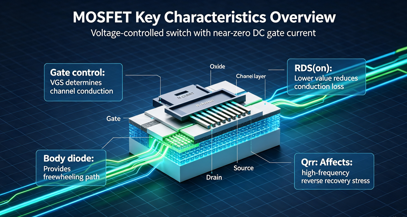
The gate electrode is isolated from the conductive channel by an oxide layer, so DC gate current is almost zero. Only transient charge and discharge current occurs during switching transitions.
Turn‑on and turn‑off speed is determined by total gate charge Qg. Larger‑current power MOSFETs require higher peak drive current to achieve fast switching speed.
Gate‑source voltage VGS governs channel conduction. Threshold voltage VGS(th) is the minimum gate‑source voltage required to build a conductive channel.
1.2 Three Operating Regions
Cut‑off Region
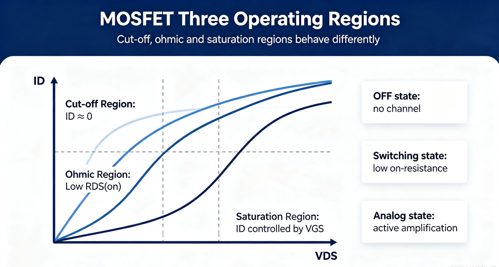
When VGS is lower than VGS(th), no conductive channel is formed. Drain current ID approximates zero and the device remains off. This corresponds to the OFF state in switching applications.
Ohmic (Linear) Region
Under the condition VGS>VGS(th) and VDS<VGS−VGS(th), the MOSFET presents low drain‑source on‑resistance RDS(on). This is the main operating region for power switching. Lower RDS(on) helps reduce conduction loss.
Saturation Region (Active Region)
When VGS>VGS(th) and VDS>VGS−VGS(th), drain current ID is primarily determined by VGS and barely affected by drain‑source voltage. This region is used for analog amplification and seldom applied for power switching.
1.3 Intrinsic Body Diode
Every power MOSFET integrates a parasitic body diode between drain and source terminals. It conducts reverse current and offers a freewheeling path for inductive loads such as BLDC motors.
Its major drawback is poor reverse‑recovery performance. It is vulnerable to failure under high‑frequency hard commutation conditions.
1.4 On‑resistance RDS(on)
RDS(on) is the drain‑source resistance when the MOSFET is fully turned‑on within the ohmic region. It directly decides conduction loss calculated as Ploss=ID2×RDS(on).
RDS(on) increases with rising junction temperature, which creates potential thermal‑runaway risks under heavy load conditions.
1.5 Breakdown Ratings
V(BR)DSS is drain‑source breakdown voltage, representing the maximum tolerable off‑state drain‑source voltage. A 30‑50 % voltage derating is required in real‑world hardware design.
VGS(max) is maximum allowable gate‑source voltage. Exceeding this rating permanently damages the thin gate oxide layer. Typical silicon MOSFETs have a ±20 V maximum VGS rating.
2. Switching Characteristics
MOSFET switching performance is restricted by internal parasitic capacitances: Cgs, Cgd also known as Miller capacitance, and Cds.
Turn‑on delay comes from charging gate capacitance up to threshold voltage. The Miller plateau is a critical phase for high‑speed design; larger Miller capacitance slows switching speed and raises switching loss. Turn‑off delay originates from gate‑charge discharging.
There exists a fundamental trade‑off: devices with lower RDS(on) usually carry higher total gate charge and larger switching loss.
3. Temperature & Thermal Characteristics
RDS(on) has a positive temperature coefficient. Multiple identical MOSFETs can be paralleled for higher‑current handling with natural current balancing, which is a key advantage over BJTs.
Junction temperature Tj must never exceed the datasheet maximum value. Thermal resistance and PCB copper pouring area dominate actual heat dissipation capability.
4. NMOS versus PMOS
NMOS uses electrons as channel carriers with higher mobility. Enhancement‑mode NMOS turns on with positive VGS, mostly deployed for low‑side switches.
PMOS relies on holes as carriers with lower mobility. Enhancement‑mode PMOS requires negative VGS to turn on and is commonly used for high‑side switching circuits.
5. Practical Design Notes
Fit appropriate gate resistors to suppress high‑frequency oscillation and limit peak gate charging current.
Never leave the gate floating. Noise can accidentally turn on the device. Pull NMOS gate down to GND and pull PMOS gate up to supply rail.
For inductive‑load circuits including BLDC motor drivers, pay close attention to body‑diode reverse‑recovery loss.
Apply sufficient voltage derating: select V(BR)DSS at least 1.5‑2 times the practical circuit operating voltage.


-

Maximizing MOSFET Output Capacitance: Advanced ...
-

Mastering MOSFET as a Switch: Complete Implemen...
-

Semiconductor Market Status of Electronic Infor...
-

How Much Instantaneous Current Is Required to T...
-

Power MOSFET V-I Characteristics: Analysis and ...
-

High Side and Low Side Drivers: Powering Modern...
-

About MOSFET driver
-

Do you know the definition of MOSFET?
-

DIY MOSFET RF Amplifier Design: A Comprehensive...
-

MOSFET Overdrive Voltage: Complete Analysis and...
-
Understand the working principle of MOSFET and ...
-

The Difference Between a Body Diode and MOSFET
-

Why the Absolute‑Value of PMOS Threshold‑Voltag...
-

How to select the most suitable driver circuit ...
-

Do you know what an N-channel MOSFET is?
-

MOSFET type and construction


