


1. Ordinary series connection (Drain‑to‑Source cascade)
Increase the overall withstand‑voltage capability. When single‑device voltage rating is insufficient, two MOS in series can share high off‑state voltage, so lower‑voltage‑rating MOS can be used for high‑voltage circuitsIEEE Xplor…. It can also implement dual‑interlock safety switch: both MOS must turn‑on simultaneously to conduct current. If either one turns off, the whole path is cut off.
- ON state: Both MOSFETs receive valid gate drive signals and turn on. Total on‑resistance equals the sum of two \(R_{DS(on)}\). Conduction loss increases.
- OFF state: Both MOS turn off. Ideally the total voltage divides across the two devices.
- Safety feature: If one MOS is damaged and stuck‑ON, the other MOS can still break the circuit for basic fault tolerance.
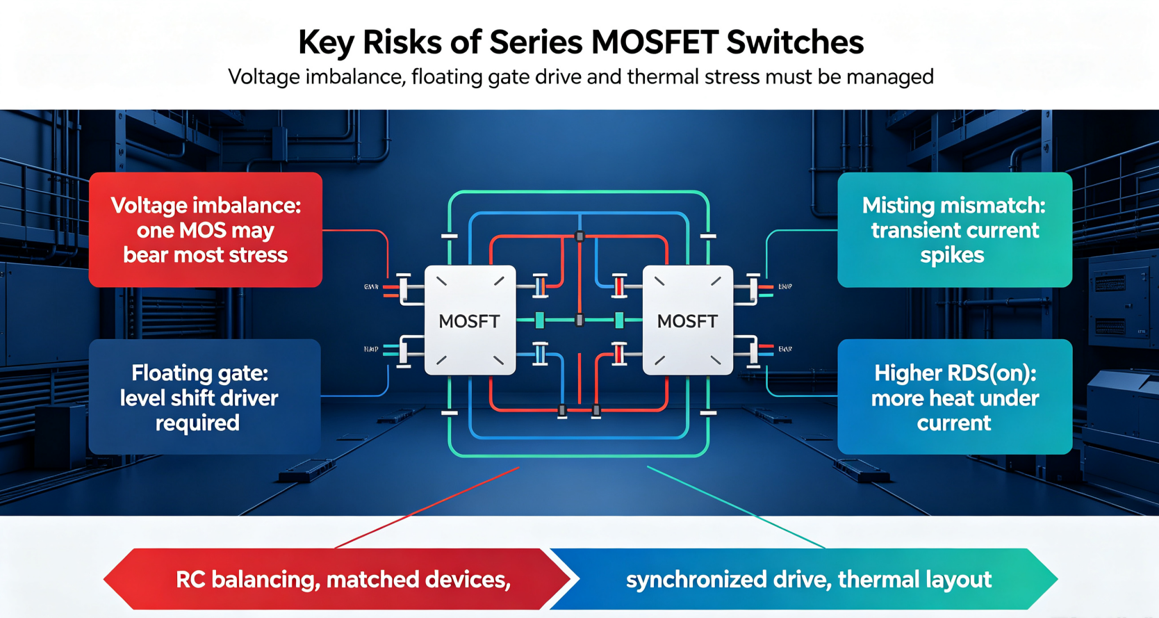
Voltage imbalance is the biggest risk. Due to difference in device parasitic capacitance, switching speed, gate‑drive delay, one MOS may bear most of the total voltage during turn‑off transient, which causes over‑voltage breakdown of that single MOS and then cascading failure of the second one. Extra voltage‑balancing RC snubber circuits are mandatory for practical high‑voltage designResearchGa….
Total conduction loss rises because two on‑resistances add together. Heat generation becomes more serious under large current.
Gate driving becomes complex. The middle floating node changes potential dynamically; direct MCU IO cannot drive floating‑side MOS without level‑shift or isolated driver.
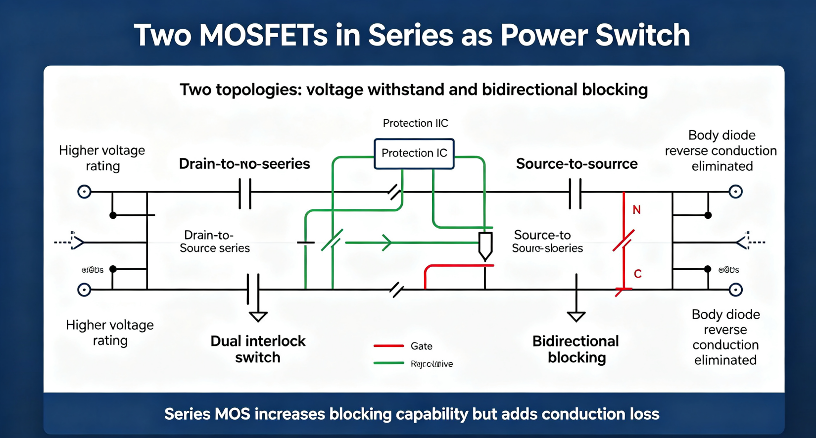
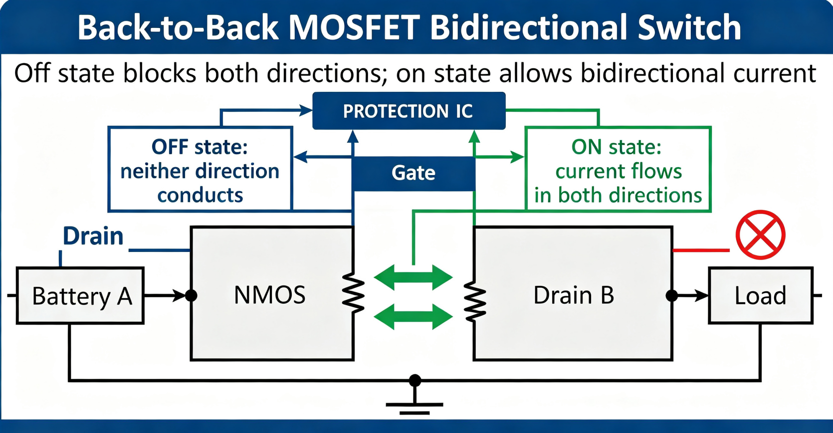
2. Back‑to‑back series (Source‑to‑Source, bidirectional switch, the one used on lithium‑ion protection board)
Solve the inherent defect of single MOSFET: the intrinsic body‑diode will conduct reverse current even when MOS channel is off. Back‑to‑back series achieves true bidirectional blocking and bidirectional controlled conduction, widely used in battery protection, AC solid‑state switch, anti‑reverse‑current circuits.
- OFF state: Both gates are low, both channels shut down. Two body diodes face opposite directions. Neither forward nor reverse current can pass through, so bidirectional voltage blocking is realized.
- ON state: Apply enough \(V_{GS}\) to both gates, both channels turn‑on. Current can flow freely in either direction between two drain terminals.
Total on‑resistance is the sum of two MOSFETs, leading to higher heating under high charging‑discharging current.
The common‑source node is floating. Gate‑source voltage references this floating node instead of ground. Direct drive from MCU IO is invalid; level‑shift gate driver is required. Timing must keep two MOS turn‑on / turn‑off synchronized. Any timing offset will produce large transient current spikes.
3. Difference between series‑MOS switch and parallel‑MOS application
3.2 Parallel MOS: main goal is higher current capacity. Voltage rating stays unchanged. Multiple devices share current; equivalent on‑resistance decreases.
4. Practical design recommendations
4.2 For bidirectional‑blocking demands such as lithium‑battery protection, select back‑to‑back source‑to‑source topology. Be sure to handle floating‑gate driving correctly.
4.3 When series connection is unavoidable: add RC voltage‑balancing networks, use devices from same production batch with consistent parameters, and strictly optimize gate‑drive timing.
4.4 Evaluate thermal budget in advance, because series‑connected MOS will bring higher conduction loss.
5. Summary
- Ordinary drain‑source series mainly boosts voltage withstand capability, but faces severe voltage imbalance risk.
- Source‑to‑source back‑to‑back series realizes bidirectional switch and eliminates body‑diode reverse‑conduction problem for battery‑protection circuits.
- Series topology brings higher total on‑resistance, more complex gate‑drive requirements and extra BOM cost. Use it only when application requirements cannot be satisfied by single‑MOS solution.


-

How Long Do MOSFETs Last? A Comprehensive Guide...
-

Analysis of the reasons for the ineffectiveness...
-
MOSFET original basic knowledge and application
-

What Happens If You Use Too‑Large Gate Resistor...
-

Complete Guide to Optocoupler MOSFET Driver Cir...
-

Analyzing Enhancement and Depletion MOSFETs
-

MPU vs MCU: Key Differences and Applications in...
-

Understanding E-MOSFET: The Building Block of M...
-
Small Package MOSFETs
-

Fast Switching MOSFETs: The Complete Guide to N...
-

What do the three pins G, S, and D of the packa...
-
What is the role of small voltage MOSFETs?
-

Market Leaders: The Most Popular MOSFETs Drivin...
-

New MOSFET Sourcing Choice: WINSOK Domestic Sub...
-
MOSFET Selection Points
-

What Are the Advantages of Power MOSFETs?


