
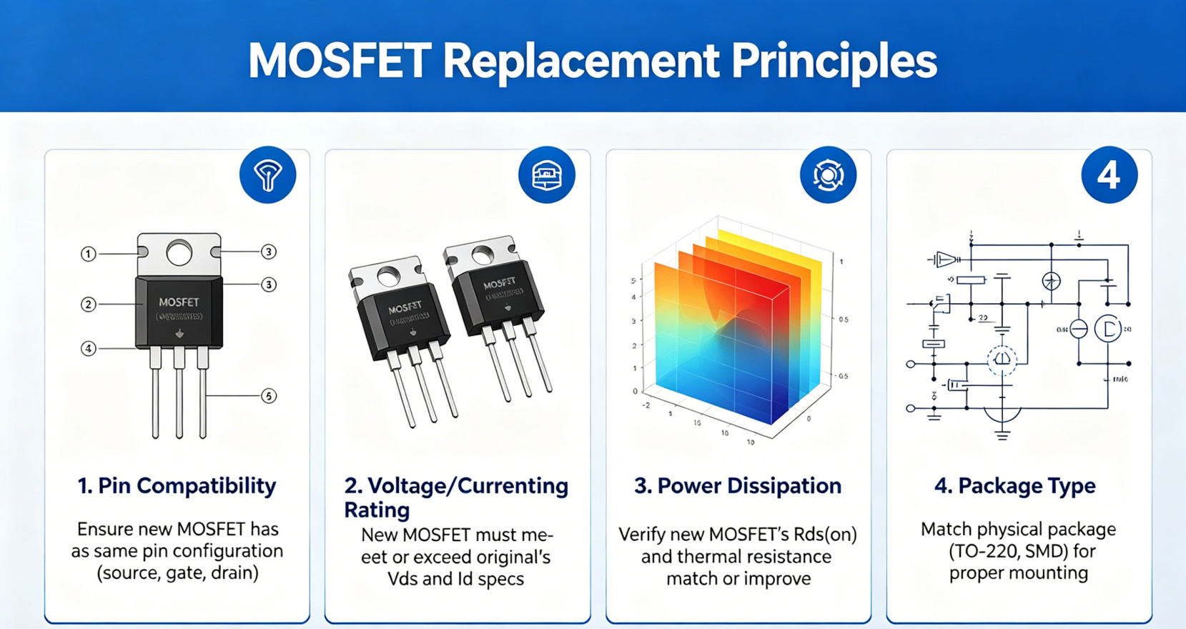
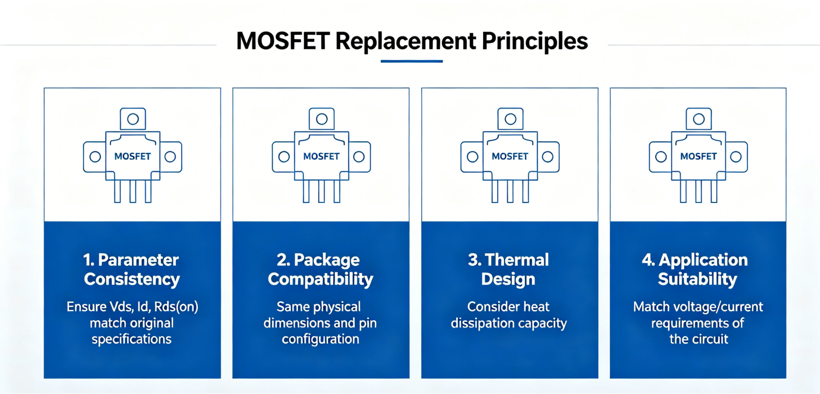
1. Primary Priority: Electrical Parameters (Most Critical)
- Channel Type Consistency
- N-channel must be replaced with N-channel, and P-channel with P-channel. They are not interchangeable. Enhancement-mode and depletion-mode types shall also be matched accordingly.
- Drain-Source Voltage (VDS)
- The VDS of the replacement MOSFET shall be no lower than that of the original component, with a margin of over 20%. Never use a device with lower VDS for low-voltage circuits.
- Maximum Drain Current (ID)
- Both continuous and pulsed drain current of the replacement part shall be greater than or equal to the original. Select a higher-rated model for high-current and power circuits.
- On-Resistance (Rds(on))
- For low-voltage & high-current circuits, the Rds(on) shall be no higher than the original value. Excessively high on-resistance will cause extra voltage drop and heat generation.
- Gate Threshold Voltage (Vgs(th))
- Match the gate drive voltage:
- Low-threshold MOSFETs for 3.3V / 5V logic drive circuits.
- Standard-threshold devices for high-voltage drive applications.
- Large deviation may lead to incomplete turn-on or false triggering.
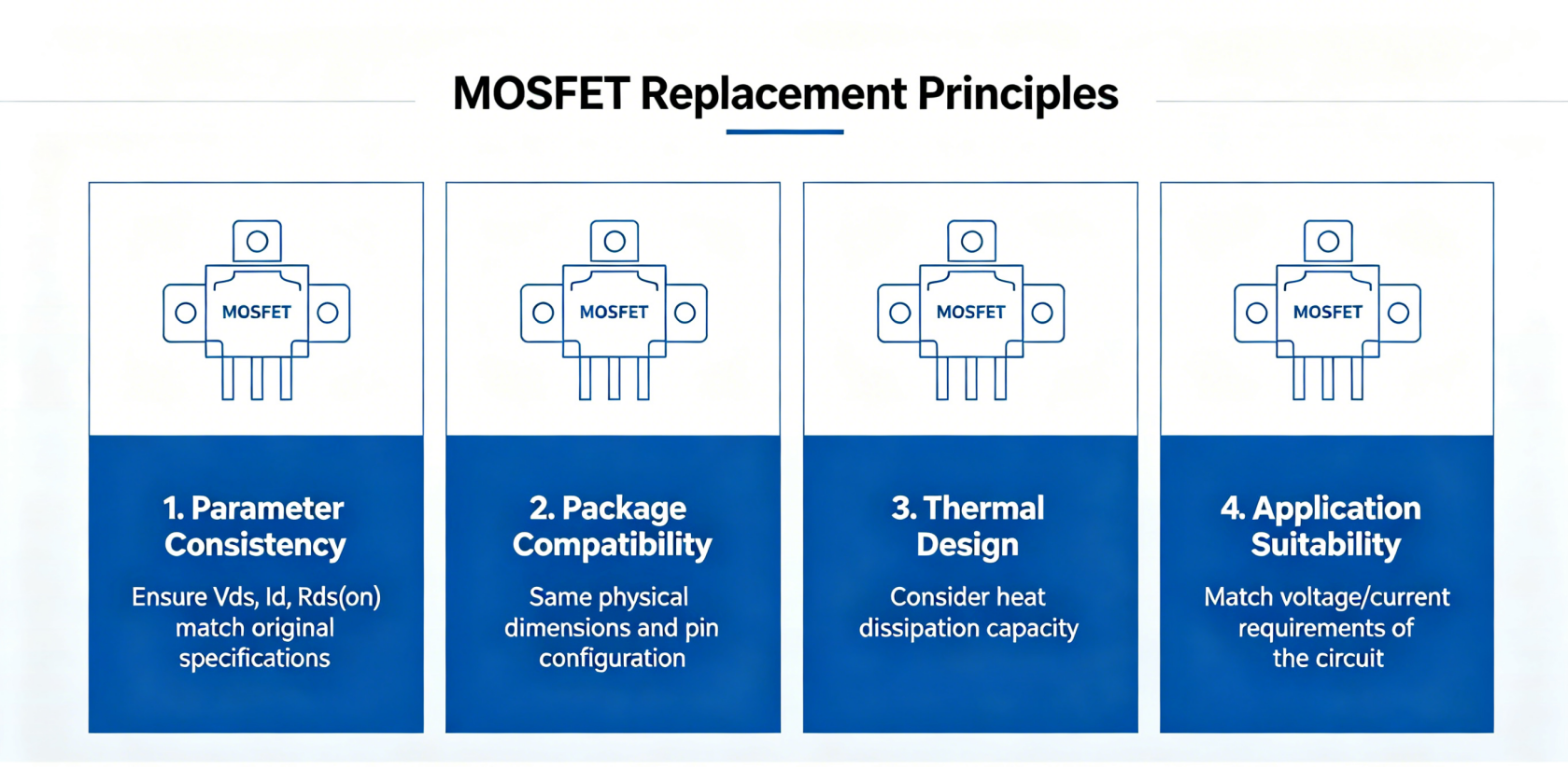
2. Secondary Priority: Package & Heat Dissipation
Use components with the same package size and pinout whenever possible to avoid PCB rewiring.
Power dissipation (Pd), maximum junction temperature (Tj) and thermal resistance (Rth) shall not be inferior to the original. For high-power applications, use identical or larger packages.
3. Switching & Driving Parameters (Mandatory for SMPS, Motor & High-Frequency Circuits)
Total Gate Charge (Qg) & Junction Capacitance (Ciss/Coss/Crss)
Keep these parameters similar for high-frequency circuits. Large differences will change switching speed, increase power loss and cause oscillation.
Switching Time (tr/tf)
Parameters must be closely matched for high-speed switching circuits; requirements can be relaxed for low-speed DC circuits.
Maximum Gate-Source Voltage (VGSmax)
It must exceed the actual drive voltage to prevent gate breakdown.
4. Rules for Different Application Scenarios
4.1 Low-Voltage DC Loads (Indicators, Simple Switches)
Basic requirements only: matched channel type, sufficient VDS and ID. Rds(on) and junction capacitance can be flexible.
4.2 High-Current / Power Paths (Power Switches, Li-ion Batteries)
Strictly control VDS, ID, Rds(on) and Pd. Prefer equivalent or upgraded specifications.
4.3 SMPS, PWM & Motor Drive (High-Frequency)
All parameters should be kept nearly identical, including VDS, ID, Rds(on), Qg, capacitance and switching time.
4.4 Analog & Signal Circuits
Prioritize devices with low junction capacitance and low drain leakage current. Parameter deviation will affect signal quality.
5. Quick Memorization Tips
Keep channel type unchanged; use equal or higher voltage/current ratings.
Focus on on-resistance for low voltage, and capacitance/charge for high frequency.
Match threshold voltage for driving; never downgrade package and heat dissipation.
6. Common Pitfalls & Notes
Drain Cutoff Current (IDSS): Keep values close for high-impedance and weak-signal circuits.
Body Diode: For freewheeling circuits, also check the reverse voltage and reverse recovery time of the body diode.
Equivalent part numbers from different manufacturers are generally interchangeable. Avoid random replacement for customized or non-standard MOSFETs.


-

2N7002 LTspice Modeling and Simulation Guide
-

Comprehensive Guide: How to Wire a MOSFET ̵...
-

Small Signal Model MOSFET Analysis and Implemen...
-

High Side and Low Side Drivers: Powering Modern...
-

How to Choose a MOSFET?
-

Understanding MOSFET’s Capacitive Propert...
-

Characteristics of Enhanced MOSFETs
-

Ideas to solve the serious heat generation of M...
-

What Is Pinch-Off Voltage in MOSFETs? Key Conce...
-

What Is the Function of MOSFET in Antenna Circu...
-

How to Measure MOSFET Power Breakdown: A Compre...
-

Advantages of MOSFETs in Motor Drive Applications
-

Four Types of MOSFETs
-

Maximizing MOSFET Output Capacitance: Advanced ...
-

Master Guide: How to Read Power MOSFET Datashee...
-

MOSFET Replacement Principles


