


1. Clarify a key point first
For enhancement‑mode devices:
- NMOS threshold voltage VGS(th) is positive, normally 0.7V‑1.0 V.
- PMOS threshold voltage VGS(th) is negative, roughly ‑0.9V ~‑1.3 V.
We actually compare absolute values. The magnitude of PMOS threshold voltage is bigger, instead of the numerical value. This difference greatly influences BLDC H‑bridge circuit design.
2. Core underlying reasons
2.1 Difference in carrier mobility (the primary cause)
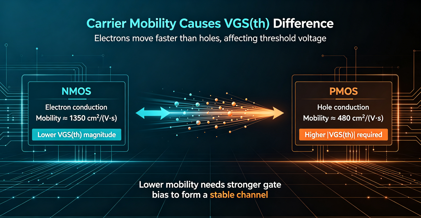
NMOS conducts by electrons, and electron mobility is about 1350 cm²/(V·s).
PMOS relies on holes for conduction, and hole mobility is only around 480 cm²/(V·s), nearly one‑third of electrons.
Under the same channel size and gate‑oxide thickness:
Holes move much harder. Chip manufacturers have to apply a higher‑magnitude gate‑source voltage to form a stable conductive channel for PMOS. If PMOS uses the same threshold‑voltage level as NMOS, the channel will be weak, and on‑resistance will rise sharply.
2.2 Different substrate structure and doping concentration
- NMOS is fabricated on a P‑type substrate.
- PMOS is built inside an N‑well which is embedded on the P‑substrate.
The N‑well brings an inherent built‑in potential difference. Higher doping concentration in the N‑well widens the depletion‑layer, which increases the voltage required to invert the channel, resulting in a larger absolute threshold‑voltage for PMOS.
2.3 Work‑function mismatch of gate material
The polysilicon gate has different work‑function values for P‑well and N‑well. This inherent material difference creates extra threshold‑voltage offset for PMOS. Even with identical silicon‑dioxide thickness, PMOS still needs higher driving‑voltage.
3. Practical impacts on BLDC‑motor design
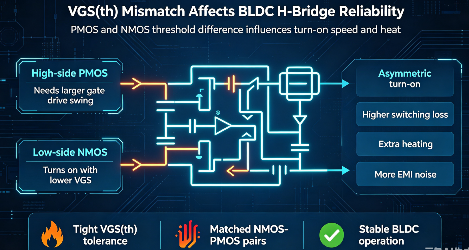
- PMOS needs a higher gate driving‑voltage to turn on fully. Insufficient gate voltage forces PMOS into the saturation region and causes serious heat generation.
- Excessive difference between PMOS and NMOS threshold‑voltage will lead to asynchronous turn‑on between high‑side PMOS and low‑side NMOS, increasing switching loss and EMI noise.
- Our Winsok‑brand PMOS strictly restricts threshold‑voltage tolerance within ±0.15 V. Matched NMOS‑PMOS pairs reduce heating and improve long‑time‑running stability for BLDC motors.

4. Brief conclusion
Low‑mobility holes, N‑well substrate and gate‑material differences lead to higher absolute threshold‑voltage of PMOS. For BLDC‑motor developers, selecting well‑matched NMOS and PMOS is critical for high‑efficiency systems.


-

Power MOSFET V-I Characteristics: Analysis and ...
-

Using a MOSFET as a Switch: Complete Implementa...
-

Small Signal Model MOSFET Analysis and Implemen...
-

What Is a Switched Mode Power Supply?
-

Understanding CMOS Switch Technology: From Basi...
-

Gate capacitance, on-resistance and other param...
-
What parameters should I pay attention to when ...
-

Why the Absolute‑Value of PMOS Threshold‑Voltag...
-

Basic MOSFET identification and testing
-

MOSFET vs FET: Why Modern Electronics Choose Me...
-

Difference Between Unipolar SPWM & Bipolar...
-

A Comprehensive Guide about What is VGS in MOSFET
-

Installing a MOSFET in Your Airsoft Gun: Step-b...
-
Commonly used SMD MOSFET package pinout sequenc...
-

VE MOSFET Technology: Revolutionizing Power Ele...
-

Why are N channel MOSFET preferred over P chann...


