


1. Circuit Structure
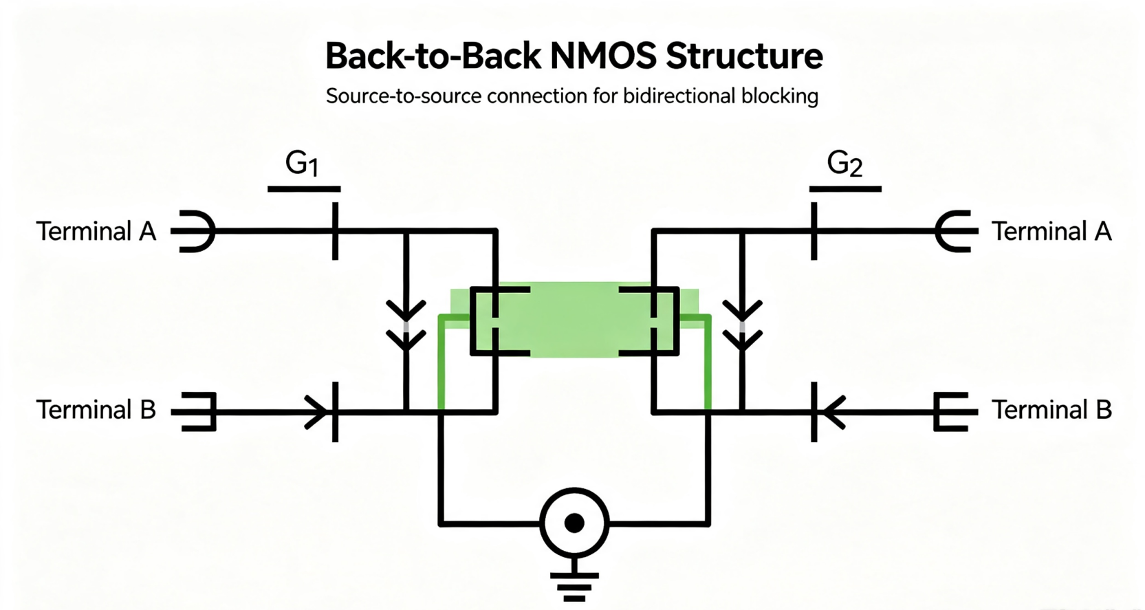
Two identical N-channel MOSFETs are connected source to source.
- - The two drain pins become the two main power terminals.
- - The two gates are driven independently.
- - The two intrinsic body diodes face opposite directions, canceling each other’s one-way conduction characteristic.
2. Working States
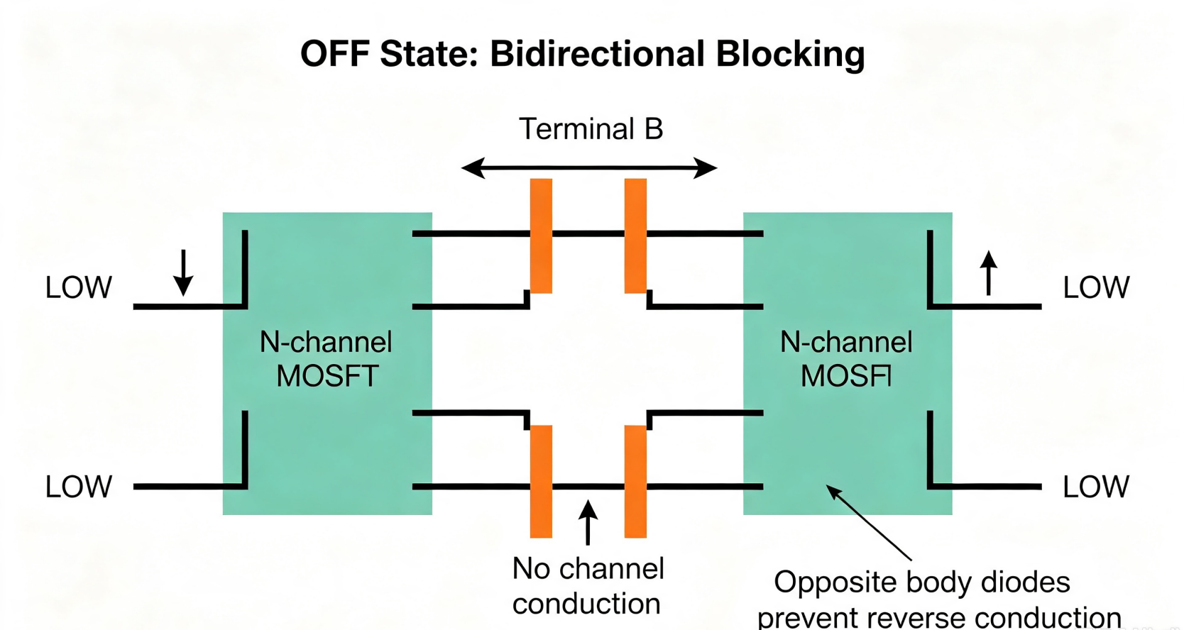
OFF State (Bidirectional Blocking)
When both gate signals are low, both MOSFET channels are closed.
No matter which direction the voltage comes from, there is no conduction path. The opposite body diodes prevent reverse leakage, achieving true bidirectional cutoff.
ON State (Bidirectional Conduction)
When both MOSFETs receive sufficient gate drive voltage, both channels turn on.
Current can flow freely in either direction between the two drain terminals. The overall on-resistance equals the series resistance of the two MOSFETs.
3. Why Not Use a Single MOSFET?
A single NMOS relies on its body diode and will always conduct in reverse voltage, which cannot block negative voltage. This causes circuit failure, reverse current leakage, and device damage.
Back-to-back NMOS eliminates this fatal defect.
4. Key Design Notes
1. The common source node is floating, so ground-referenced MCU signals cannot directly drive the gates. A level-shift gate driver is required.
2. Both MOSFETs must be turned on or off simultaneously to avoid asymmetric stress.
3. This structure increases total on-resistance, so low Rds(on) MOSFETs are recommended for high-current applications.
5. Typical Applications
- Battery reverse polarity protection
- Bidirectional DC power switches
- AC small signal switching circuits
- BLDC bidirectional current control systems
6. Summary
Back-to-back source-to-source NMOS is the standard solution for bidirectional voltage blocking. It solves the reverse conduction problem of the MOSFET body diode and is essential for reliable reverse protection and AC switching designs.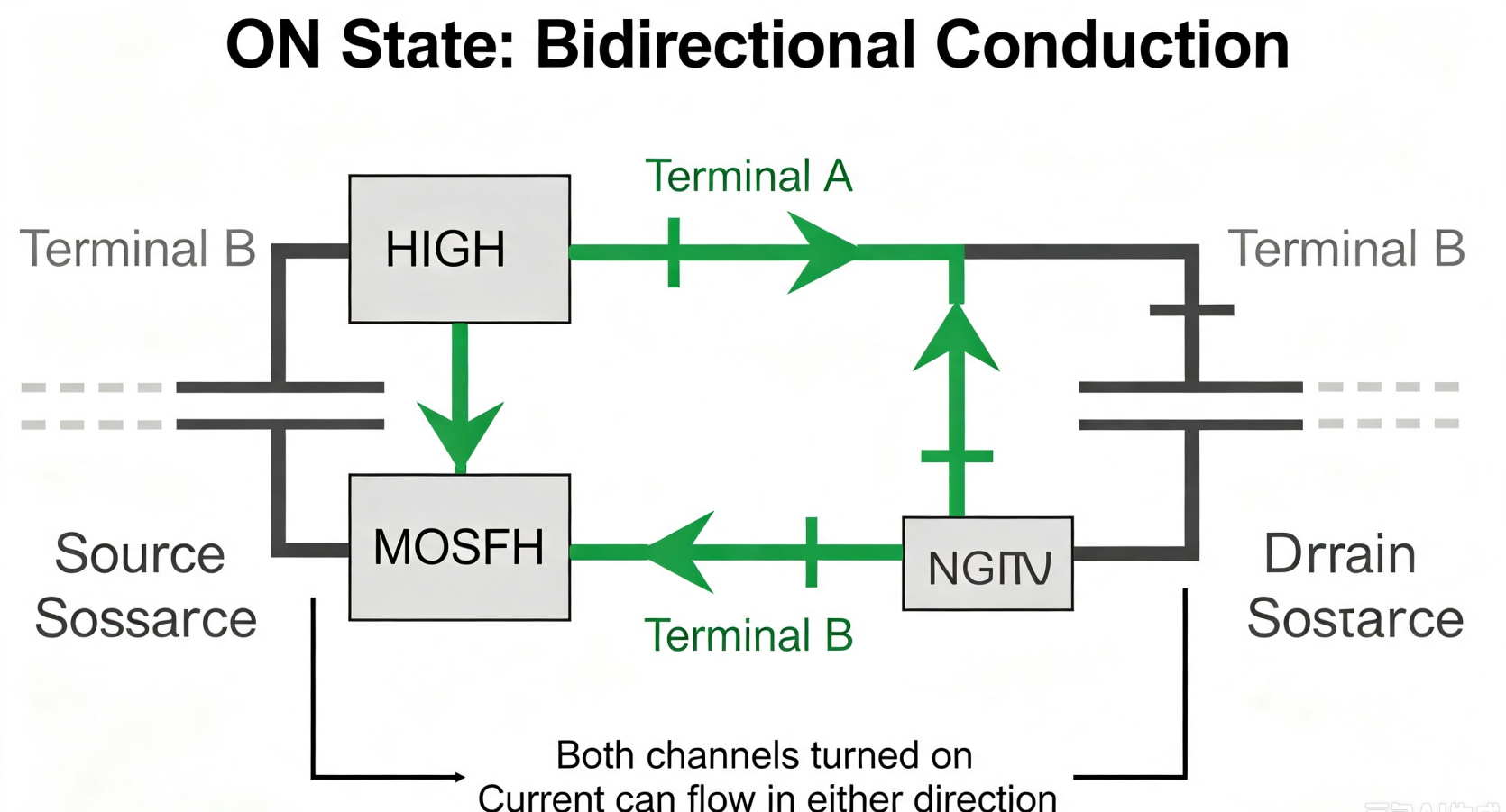


-

What Are the Advantages of Power MOSFETs?
-
What is the role of small voltage MOSFETs?
-

The Complete Guide to MOSFET Gate Resistors: Se...
-

About MOSFET driver
-

Determining MOSFET Threshold Voltage: Expert Te...
-

Understanding the Operation and Modeling of MOS...
-

Understanding MOSFET Switching Speed for Optima...
-

MOSFET Gate, Drain, and Source: Core Principles...
-

New MOSFET Sourcing Choice: WINSOK Domestic Sub...
-

Which brand of MOSFET is good
-

Understanding MOSFET Overdrive Voltage: Compreh...
-

How to select the most suitable driver circuit ...
-

Gate capacitance, on-resistance and other param...
-

How to Evaluate MOSFET Performance Parameters D...
-

MOSFET gate source protection
-

Analysis of the reasons for the ineffectiveness...


