
Core Procedures and Key Points for MOSFET Selection
Select MOSFETs step by step based on circuit operating conditions, electrical parameters and application scenarios, prioritizing performance, stability and cost.
1. Confirm Application Scenarios and Circuit Topology First
Clarify the circuit type to narrow down the basic selection range:
- 1:Switching Circuits (DC-DC converters, relay drivers, load switches): Prioritize switching speed and on-state loss.
- 2.Linear Amplifier & Analog Circuits: Focus on transconductance, linear region characteristics and low noise performance.
- 3.Power Conversion Circuits (inverters, charging piles, motor drivers): Emphasize voltage rating, current capacity, heat dissipation and surge resistance.
- 4.Low-Voltage Signal Circuits (board-level small signal systems): Select devices with low threshold voltage, compact package and low leakage current.
Distinction between N-channel and P-channel MOSFETs:
- N-channel MOSFET: The mainstream choice, featuring lower on-resistance. Ideal for low-side switches, lower arms and ground-referenced switching.
- P-channel MOSFET: Simple to drive, commonly used for high-side switches on the power rail. Rarely adopted in high-voltage and high-current applications.
2. Selection Based on Core Electrical Parameters
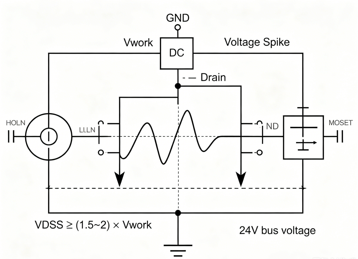
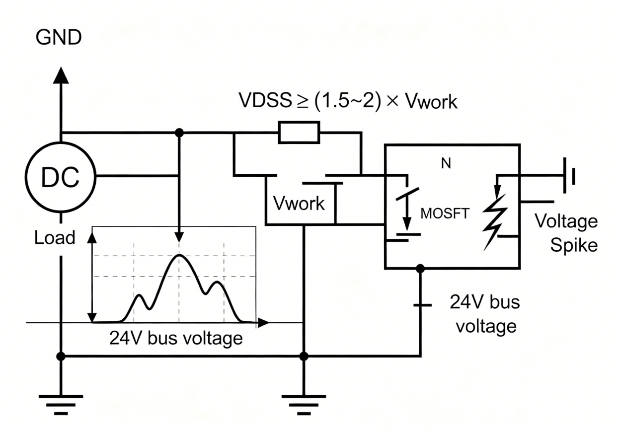
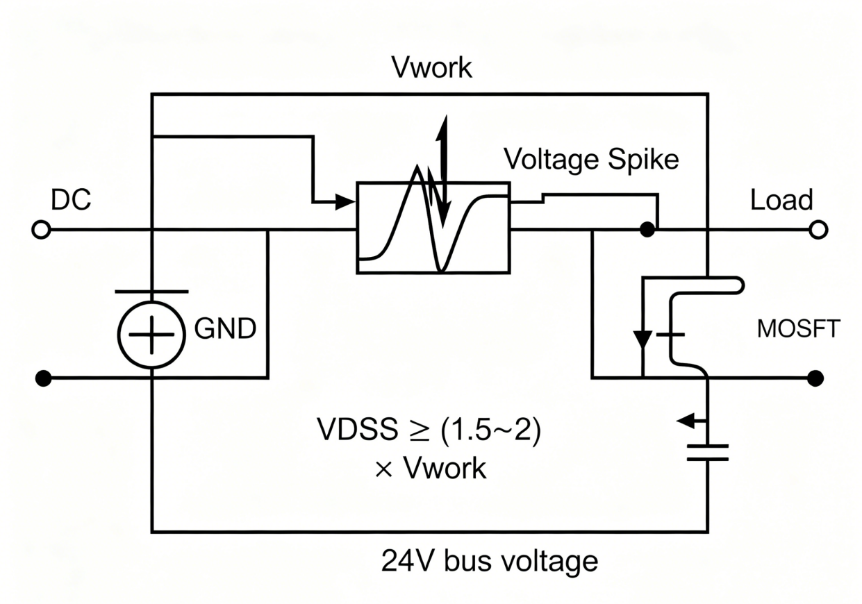
(1) Drain-Source Voltage Rating (\(V_{DSS}\))
- Rule of thumb: The rated \(V_{DSS}\) shall be 1.5 to 2 times the maximum operating voltage of the circuit to withstand surges and voltage spikes
- Example: For a 24 V bus voltage, choose MOSFETs with \(V_{DSS} \ge 40\ \text{V}\); for a DC voltage of approximately 310 V after 220 V rectification, select 600 V / 650 V rated devices.
- For high-voltage applications, pay special attention to avalanche withstand capability to prevent breakdown caused by voltage spikes.
(2) Continuous Drain Current (\(I_D\))
- The rated \(I_D\) must exceed the maximum steady-state operating current. Derate the current by 30% to 40% considering temperature rise for power circuits.
- Check the pulse drain current (\(I_{DM}\)) for transient peak current conditions.
- Choose small-signal MOSFETs for mA-level low-current circuits, and power MOSFETs or parallel configurations for high-current applications (tens of amperes and above).
(3) On-Resistance (\(R_{DS(on)}\))This parameter determines conduction loss and is critical for low-voltage high-current circuits.
- For 5 V / 12 V / 24 V low-voltage systems, prioritize devices with low \(R_{DS(on)}\) to reduce heat generation.
- Note: \(R_{DS(on)}\) increases as junction temperature rises. Refer to the temperature drift curve in the datasheet for high-temperature operating conditions.
- Within the same package, a lower \(R_{DS(on)}\) means a larger die size and higher cost.
(4) Gate Threshold Voltage (\(V_{GS(th)}\))
- Standard threshold (2 ~ 4 V): Compatible with conventional 3.3 V / 5 V MCU driving circuits.
- Low threshold (around 1 V): Suitable for 1.8 V low-voltage logic drive.
- Ensure the driving voltage is higher than \(V_{GS(th)}\); otherwise, the MOSFET cannot be fully turned on.
- Check the maximum gate-source voltage (\(V_{GS(max)}\), typically ±20 V). Add clamping protection in the drive circuit to avoid overvoltage damage.
(5) Switching Parameters (Essential for Switching Circuits)These parameters affect switching loss, EMI and operating frequency.
- Total gate charge (\(Q_G\)), input capacitance (\(C_{iss}\)), output capacitance (\(C_{oss}\)) and reverse transfer capacitance (\(C_{rss}\)): Smaller values deliver faster switching speed and lower high-frequency loss.
- Rise time, fall time and tail time are key indicators for high-frequency DC-DC converters and RF circuits.
- Requirements for switching parameters can be relaxed for circuits operating below 10 kHz.
3. Body Diode Characteristics (Critical for Inductive Loads)A built-in body diode is integrated inside each MOSFET, which plays a freewheeling role for inductive loads such as inductors, motors and relays.
- Verify the forward current rating and reverse recovery time (\(t_{rr}\)) of the body diode for inductive switching circuits.
- Select MOSFETs with fast-recovery body diodes for high-frequency operation to cut down reverse recovery loss.
- If the body diode cannot meet requirements under high voltage and large current, connect an external Schottky diode in parallel.
4. Package and Heat Dissipation Matching
- Small-signal & low-current applications: SOT-23, SOT-323 (miniature packages without extra heat sinks).
- Medium-power applications: SOP-8, DFN (heat dissipation via enlarged copper pads on PCB).
- High-power applications: TO-220, TO-247, TOLL (matched with dedicated heat sinks).
- Refer to thermal resistance (\(R_{th(jc)}\)): Lower thermal resistance means better heat dissipation and higher operational stability at high temperatures.
5. Temperature Performance and Reliability
- Standard operating junction temperature range: -55 °C ~ +150 °C. Choose wide-temperature models for harsh high-temperature environments.
- Conduct temperature rise simulation or actual testing for long-term operation to avoid exceeding the maximum junction temperature.
- For automotive and industrial applications, select automotive-grade or industrial-grade MOSFETs with enhanced anti-interference and temperature stability.
6. Selection for Special Application Scenarios
- High-voltage fast charging & inverter systems: Adopt SiC MOSFETs (Silicon Carbide MOSFETs). They feature high voltage resistance and far lower switching loss than traditional silicon MOSFETs.
- Ultra-low power standby systems: Choose devices with low drain leakage current (\(I_{DSS}\)) to minimize static power consumption.
- Parallel current sharing circuits: Use MOSFETs from the same production batch with consistent parameters, and adopt dedicated current sharing designs.
- Systems with strict EMC requirements: Select devices with matched junction capacitances and gentle switching edges to reduce electromagnetic radiation.
Summary of Simplified Selection Process
- Define circuit topology, channel type (N/P), operating voltage, current and frequency.
- Select \(V_{DSS}\) and \(I_D\) with a 1.5~2x derating margin.
- Match \(V_{GS(th)}\) with drive voltage, and select proper \(R_{DS(on)}\) based on power consumption.
- Prioritize gate charge and capacitance for high-frequency circuits; evaluate body diodes for inductive loads.
- Determine package type and heat dissipation solution according to current and power dissipation.
- Finally confirm cost, supply availability and device grade (consumer / industrial / automotive).


-

How to prevent MOSFET failure
-

Semiconductor Market Status of Electronic Infor...
-
WINSOK|China e-Hotspot Solution Innovation Summ...
-
How to choose MOSFET?
-

Power MOSFET V-I Characteristics: Analysis and ...
-

Guidelines for MOSFET Package Selection
-

MOSFET as Ideal Diode: Revolutionary Approach t...
-

MOSFET Selection | N-Channel MOSFET Constructio...
-

Original spot CMS79F726 package SOP20 touch but...
-

Detailed explanation of the working principle o...
-

Testing MOSFETs on PCBs: Field Testing Methods ...
-

DIY MOSFET RF Amplifier Design: A Comprehensive...
-

MPU vs MCU: Key Differences and Applications in...
-

Floating Gate MOSFET Implementation: Key Steps ...
-

Why the Absolute‑Value of PMOS Threshold Voltag...


