
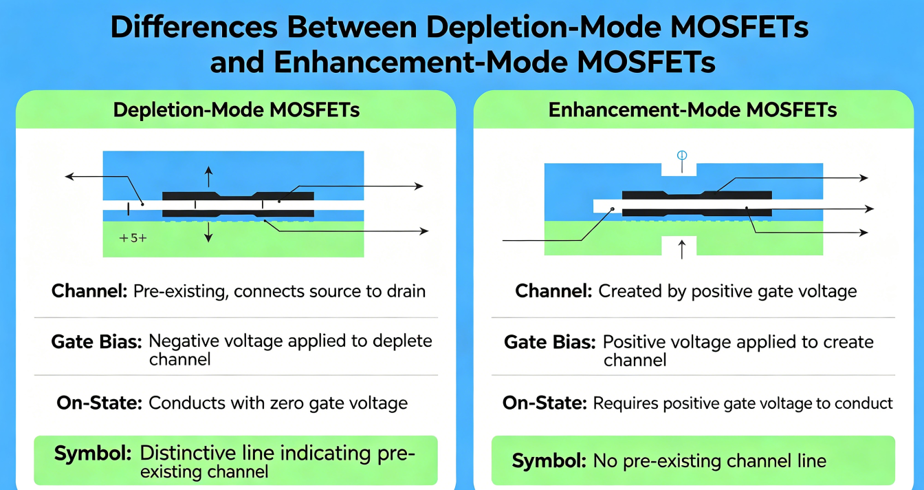
Differences Between Depletion-Mode MOSFETs and Enhancement-Mode MOSFETs
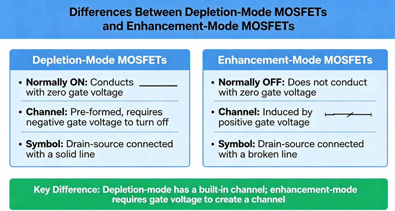
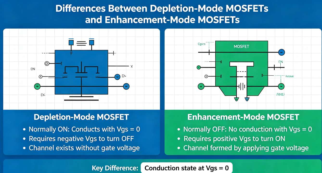
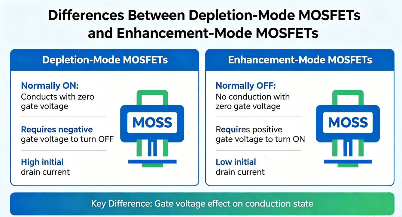
1. Fundamental Difference (Conduction State at Zero Gate Bias)
(1) Enhancement-Mode MOSFET (E-MOSFET)
- When gate-source voltage \(V_{GS}=0\), the conductive channel is fully disconnected with nearly zero drain current.
- No inherent conductive channel exists on the substrate. An external gate voltage must be applied to induce a conductive channel for turn-on.
- Naming origin: The applied voltage enhances conductivity; the device stays off with zero gate bias.
(2) Depletion-Mode MOSFET (D-MOSFET)
- When gate-source voltage \(V_{GS}=0\), a pre-fabricated inherent conductive channel exists, generating drain current \(I_{DSS}\).
- Impurities are ion-implanted into the substrate during manufacturing to form a permanent conductive channel.
- A reverse gate voltage must be applied to deplete charge carriers in the channel and switch the device off.
2. Comparison of Gate-Source Voltage Polarity (N-channel / P-channel)
N-channel (Most Widely Used)
N-channel Enhancement-Mode MOSFET (NMOS)
- Turn-on condition: \(\boldsymbol{V_{GS} > V_{GS(th)}}\)
- \(V_{GS(th)}\) = positive threshold voltage
- \(V_{GS}=0\): Cutoff state, \(I_D≈0\)
- Applications: Low-voltage logic chips, power switching MOSFETs for power supplies
N-channel Depletion-Mode MOSFET
- Conductive under zero gate bias with measurable \(I_{DSS}\). Operates with both positive and negative gate voltages:
- \(V_{GS}>0\): Channel widens, drain current rises
- \(V_{GS}<0\): Channel depletes, drain current drops
- Turn-off condition: \(\boldsymbol{V_{GS} < V_{GS(off)}}\)
- \(V_{GS(off)}\) = negative pinch-off voltage
- Applications: RF amplifiers, constant current sources, signal biasing circuits
P-channel DevicesP-channel Enhancement-Mode MOSFET (PMOS)
- Turn-on condition: \(V_{GS} < V_{GS(th)}\)
- \(V_{GS(th)}\) = negative threshold voltage; cutoff at zero gate bias.P-channel Depletion-Mode MOSFETConductive with zero gate bias. A positive gate voltage depletes the channel to cut off the device; its \(V_{GS(off)}\) is positive.
3. Comparison Table of Key Parameters
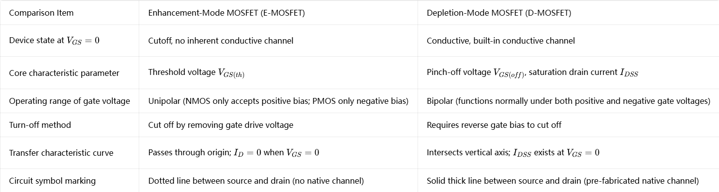
- Comparison ItemEnhancement-Mode MOSFET (E-MOSFET)Depletion-Mode MOSFET (D-MOSFET)Device state at \(V_{GS}=0\)Cutoff, no inherent conductive channelConductive, built-in conductive channelCore characteristic parameterThreshold voltage \(V_{GS(th)}\)Pinch-off voltage \(V_{GS(off)}\), saturation drain current \(I_{DSS}\)Operating range of gate voltageUnipolar (NMOS only accepts positive bias; PMOS only negative bias)Bipolar (functions normally under both positive and negative gate voltages)Turn-off methodCut off by removing gate drive voltageRequires reverse gate bias to cut offTransfer characteristic curvePasses through origin; \(I_D=0\) when \(V_{GS}=0\)Intersects vertical axis; \(I_{DSS}\) exists at \(V_{GS}=0\)Circuit symbol markingDotted line between source and drain (no native channel)Solid thick line between source and drain (pre-fabricated native channel)
4. Brief Explanation of Transfer Characteristic Curves
N-channel Enhancement-Mode MOSFET
Drain current \(I_D\) only emerges when \(V_{GS}\) exceeds the positive threshold voltage; no current at the origin.
N-channel Depletion-Mode MOSFET
The vertical axis intercept at \(V_{GS}=0\) represents \(I_{DSS}\).
Current decreases as voltage shifts negative, falling to zero at \(V_{GS(off)}\); current rises continuously with positive gate bias.
5. Typical Application Scenarios
Enhancement-Mode MOSFETs (Dominant in Most Circuits)
- Digital logic: CPUs, MCUs, CMOS logic gates (paired NMOS & PMOS enhancement-mode devices)
- Power switches, DC-DC converters, motor drivers, load switches
- High-power MOSFETs, SiC MOSFETs, auxiliary switching devices for IGBTs
- Advantages: Simple control, auto-cutoff at zero gate bias, straightforward drive circuitry, high operational safety.
Depletion-Mode MOSFETs (Specialized for Analog Circuits)
- High-frequency RF & microwave amplifiers
- Precision constant current sources, active loads
- Simplified biasing circuits (operate directly at \(V_{GS}=0\) without extra gate power supply)
- High-input-impedance signal buffers
- Advantages: Bipolar gate voltage operation, built-in quiescent current, ideal for small-signal analog processing.
- Disadvantages: Not suitable for high-power switching applications.
6. Quick Identification via Circuit Symbols
- Enhancement-mode: Dotted line between source and drain (indicates no native conductive channel)
- Depletion-mode: Solid thick line between source and drain (indicates pre-implanted permanent conductive channel)
7. One-Sentence Summary
- Enhancement-mode MOSFET: Cut off with zero gate bias, turns on only with applied voltage; used as electronic switches and digital logic components.
- Depletion-mode MOSFET: Remains conductive with zero gate bias, requires reverse voltage to turn off; widely adopted in analog amplifiers and constant current sources.
- Glossary (Professional Terms)
- MOSFET: Metal-Oxide-Semiconductor Field-Effect Transistor
- Enhancement-mode:
- Depletion-mode:
- Threshold voltage (\(V_{GS(th)}\)):
- Pinch-off voltage (\(V_{GS(off)}\)):
- Saturation drain current (\(I_{DSS}\)):
- Conductive channel:
- Transfer characteristic:
- Cutoff / Turn-off:
- Gate-source voltage (\(V_{GS}\)):


-

High Side and Low Side Drivers: Powering Modern...
-

Analysis of the reasons for the ineffectiveness...
-

MOSFET Solid State Relay Circuits: Revolutionar...
-
MOSFET Selection Points
-

The Complete Guide to MOSFET Gate Resistors: Se...
-

MOSFET Failure Analysis: Understanding, Prevent...
-

What Is JFET and MOSFET? Transistors that Power...
-

MOSFET in Airsoft: Revolutionizing Performance ...
-

Flow of MOSFET testing
-

MOSFET overview
-

EV dashboards are prone to break down, maybe it...
-

What are the main features of MOSFETs?
-

Detailed explanation of the working principle o...
-
Olukey explains the parameters of MOSFET for you!
-

Original spot CMS79F726 package SOP20 touch but...
-

What is TTL Logic: A Comprehensive Guide to Tra...


