


High-voltage MOSFETs (typically >200V, super-junction MOSFET widely used) cannot be directly driven by MCU GPIO pins. The floating high-side node, large gate charge Qg, strong Miller effect and high dv/dt are the main design challenges. A proper gate drive circuit is critical to avoid false turn-on, suppress oscillation, balance switching loss and EMI.
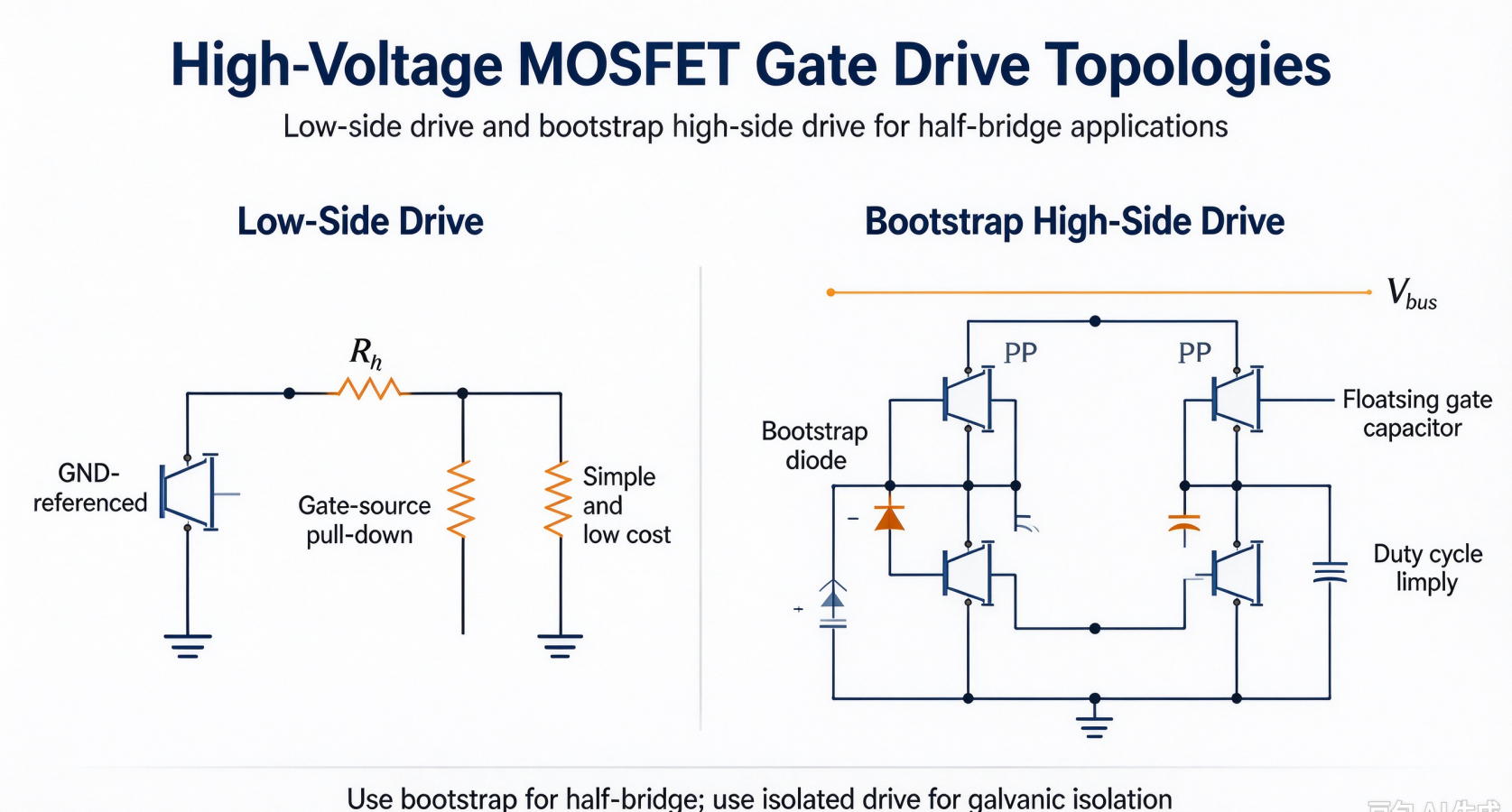
1. Low-side Gate Drive (Simplest Topology)
Low-side MOSFET means source pin connected to power GND. The gate potential is referenced to ground, so the drive design is easier.
- Direct dedicated gate driver IC or discrete push-pull buffer.
- Series gate resistor Rg to control switching speed; anti-parallel diode for faster turn-off.
- Gate-source pull-down resistor (10k~100k): keeps Vgs=0 when driver is floating, prevents accidental turn-on.
Pros: Simple, low cost, easy layout.
Cons: Only works for low-side switches; not applicable for half-bridge, totem-pole high-side.
Typical applications: Flyback, buck converter low-side switch.
2. Bootstrap High-Side Drive (Most Popular Non-isolated)
For half-bridge / totem-pole topologies, high-side MOSFET source floats and swings between GND and high DC bus voltage. Bootstrap circuit uses bootstrap diode and bootstrap capacitor to generate a floating supply for high-side driver.
- Bootstrap capacitor charges during low-side ON time. It supplies gate charge to turn the high-side MOSFET ON.
- Limitation: cannot run at 100% duty cycle. Minimum off-time is required to recharge the bootstrap capacitor.
- Key design points: low ESR bootstrap cap, fast recovery bootstrap diode, careful VS spike suppression.
Pros: Single supply, fewer components, low cost for half-bridge.
Cons: Duty cycle limitation, vulnerable to large VS undershoot.
Typical applications: Half-bridge LLC, BLDC motor drivers.
3. Isolated Gate Drive (Opto / Capacitive Isolation)
When galvanic isolation is required between control logic and high voltage power rail, use isolated gate drivers.
- Optocoupler gate driver: opto transmits PWM signal, secondary side provides gate charging current.
- Capacitive isolated driver (digital isolator + gate buffer): faster speed, lower propagation delay than optocoupler.
- The secondary side needs an isolated auxiliary power supply.
Negative gate bias (-5V commonly) is highly recommended for high dv/dt systems. Negative Vgs greatly suppresses Miller-induced self-turn-on.
Pros: Full galvanic isolation, high noise immunity, no duty cycle limit.
Cons: Higher BOM cost, more PCB area.
Typical applications: Offline high voltage converters, industrial power, medical power supply.
Critical Design Rules for HV MOSFET Gate Drive
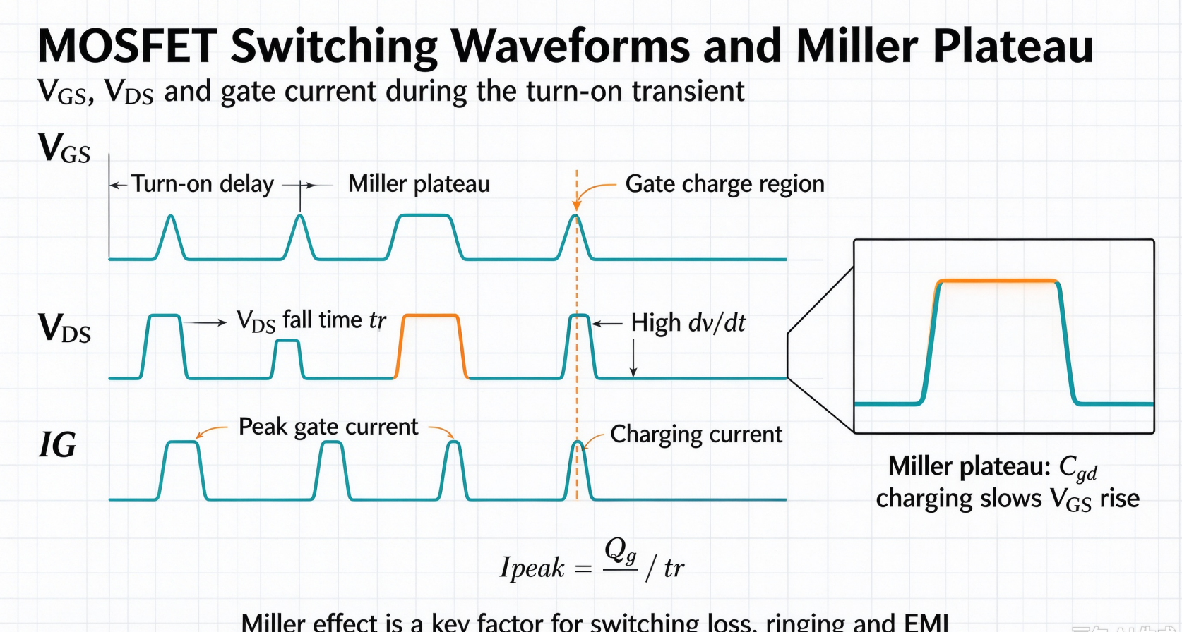
- Sufficient peak gate current: Ipeak = Qg / tr. High voltage super-junction MOSFET has large Qg; weak drive leads to slow switching and huge heat.
- Rg split (Rg_on ≠ Rg_off): Separate resistor and diode network. Moderate Rg_on reduces EMI and voltage spike; smaller Rg_off for fast discharge of gate charge.
- Miller clamp: A dedicated Miller clamp pin on some driver ICs pulls gate hard to source during Miller plateau, stopping false turn-on.
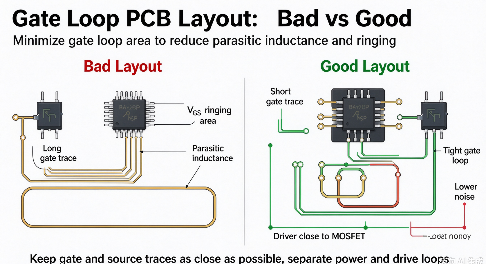
- PCB layout rule: Gate loop must be as short as possible. Gate and source traces form a tiny loop; parasitic inductance causes ringing and Vgs overshoot.
- UVLO protection: Undervoltage lockout prevents operating MOSFET in linear region. If drive voltage is insufficient, MOSFET stays in the resistive zone and burns out quickly.
Summary
Choose low-side drive for ground-referenced switches. Bootstrap is the cost-effective pick for half-bridge when 100% duty cycle is not needed. Isolated gate driver with negative bias is the robust choice for high-voltage offline and industrial systems. Always match peak gate current, tune Rg and optimize gate loop layout to handle Miller effect and dv/dt transients.


-

How to Choose a MOSFET: The Complete Selection ...
-

Difference between output power MOSFET and bipo...
-

Best Places to Source Quality MOSFET Transistor...
-
Main parameters of MOSFETs and comparison with ...
-

Differences Between IGBT and MOSFET
-

Building a MOSFET H-Bridge: Essential Guide for...
-

Wiring a MOSFET for Your Nerf Blaster: Professi...
-

Why the Absolute‑Value of PMOS Threshold Voltag...
-
Application of MOSFET in the drive circuit of D...
-

Which brand of MOSFET is good
-

Analysis of important causes of MOSFET heat gen...
-

How to Choose a MOSFET?
-

What Is MCU in Electronics: The Brain Behind Sm...
-

Understanding E-MOSFET: The Building Block of M...
-

Building OR Gates Using MOSFETs: A Practical Im...


