
IGBTs are widely adopted in high-power audio power amplifiers (mostly Class D / H-bridge topologies).
Their dedicated circuit designs mainly focus on high-voltage & high-current driving, galvanic isolation, precise dead-time control, snubber circuits, fast overcurrent/short-circuit protection, high-voltage LC filtering and thermal management, which differ greatly from MOSFET-based amplifiers.
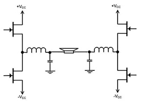
1. Topology: H-Bridge / Full-Bridge for High Voltage & High Power IGBTs are ideal for systems with 300–800 V high DC bus voltage, 50–500 A large current and operating frequencies below 20 kHz, so full-bridge (H-bridge) is the mainstream topology instead of the half-bridge commonly used with MOSFETs.
- Linear Amplifier (OCL/OTL): Rare application
- When IGBTs are used in output stages, a fixed voltage bias circuit is required to eliminate crossover distortion, with quiescent current set to 50–100 mA.
- Class D Switching Amplifier (Mainstream)
- A 4-IGBT H-bridge structure with PWM modulation is adopted. It achieves efficiency over 90% and is suitable for professional audio and industrial drivers with power ranging from 1 kW to 100 kW.
2:Gate Drive Circuit: High-Current Drive + Negative Turn-Off + Isolation (Core Part)IGBTs feature large gate charge and a maximum gate voltage rating of ±20 V. The drive circuit must deliver sufficient peak current, apply negative voltage for reliable turn-off and provide galvanic isolation — these are distinct from MOSFETs which typically use +10 V drive without negative bias.
- Matched Drive Voltage
- Turn-on: +15 V (±5%) to ensure full saturation and low on-state loss (typical \(V_{CE(sat)}\): 1.8–2.5 V).
- Turn-off: -5 V ~ -8 V (mandatory). It quickly discharges gate charge, suppresses the Miller effect and prevents false turn-on, especially critical for high-voltage systems.
- Gate protection: Install a bidirectional TVS (±18 V) in close proximity for voltage clamping. A power resistor of 5–10 Ω is connected in series with the gate to suppress ringing and balance switching speed and EMI performance.
- High Peak Drive Current
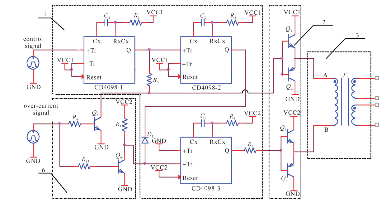
- The total gate charge \(Q_G\) of IGBTs ranges from 100 nC to 500 nC, so the drive circuit needs a peak current ≥ 2–5 A. Dedicated IGBT drive ICs (e.g. IR2110, IR2113, Infineon EVAL-IGBT series) or discrete totem-pole circuits are recommended.
- Mandatory Galvanic Isolation
- Isolate the high-voltage power stage (300 V+) from the low-voltage control stage (15 V). Use high CMTI optocouplers (e.g. 6N137) or magnetic isolators (e.g. ADI ADuM1400) with isolation voltage ≥ 2.5 kV. Independent isolated auxiliary power supplies are required to avoid common-ground interference.
3. Dead-Time Control: Precise Delay to Prevent Shoot-ThroughThe upper and lower devices in half-bridge / H-bridge topologies must never conduct simultaneously.
- IGBTs have a relatively long turn-off storage time (1–3 μs), so a longer dead time is required.
- Fixed dead time: 2–5 μs (0.5–1 μs for common MOSFET designs).
- Dynamic dead time (high-end design): Compensate dead time against temperature and load current. Extend dead time automatically as temperature or current rises (e.g. +10 ns per °C, +50 ns per 10 A) to balance safety and efficiency.
- Hardware interlock: PWM signals are verified by dedicated ASIC or FPGA logic to block shoot-through caused by software faults.
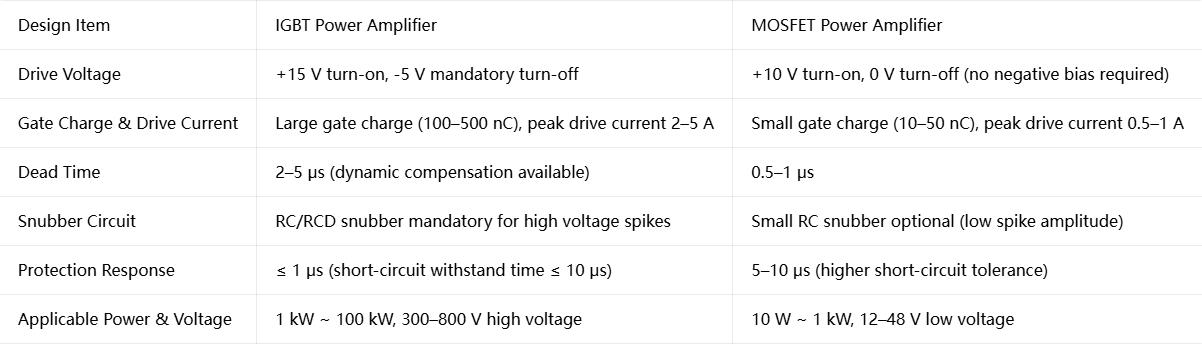
4. Snubber Circuit: Suppress High-Voltage SpikesParasitic inductance on power lines will induce severe \(V_{CE}\) voltage spikes (up to twice the DC bus voltage) during switching. RC / RCD snubbers are essential.
- RC Snubber (General use): Connect a 10 Ω / 2 W resistor in series with a 1 nF / 1 kV capacitor across the collector and emitter of each IGBT to absorb voltage spikes and suppress oscillation.
- RCD Snubber (High power > 50 kW): Add a fast recovery diode for more efficient energy absorption.
- DC bus snubber: Parallel low-ESR electrolytic capacitors and film capacitors on the main DC bus to stabilize bus voltage.
5. Protection Circuit: Microsecond-Level ResponseIGBTs have extremely short short-circuit withstand time (≤ 10 μs), so protection circuits must respond extremely fast and reliably.
- Overcurrent & Short-Circuit Protection (Key)
- Sensing: Use precision shunt resistors (0.01–0.1 Ω) or Hall sensors to collect collector current signals.
- Response: High-speed comparators work with drive ICs to hard shut down the gate within 1 μs. Desaturation detection (monitoring rising \(V_{CE}\) under short circuit) is also adopted, a built-in function of dedicated IGBT drive chips.
- Overvoltage Protection
- Install MOVs or gas discharge tubes on the DC bus for surge absorption. TVS diodes with rated voltage 1.5 times the bus voltage are connected across IGBT terminals for spike clamping.
- Over-Temperature Protection
- Mount NTC thermistors on heat sinks to cut off output when temperature reaches 100–120 °C. High-power IGBT modules integrate built-in temperature sensors for direct connection to drive circuits.
6. Output Filter: High-Voltage Low-Pass LC Filter for PWM SignalsThe output of Class D amplifiers is high-frequency PWM waves (200 kHz–1 MHz). A dedicated low-pass filter is needed to restore audio signals.
- Topology: 2nd-order LC filter or π-type LC filter, cut-off frequency set to 20–50 kHz.
- Inductor: High-current coreless or powder core inductors (50–200 μH, 50–500 A) with anti-saturation and low-loss characteristics.
- Capacitor: High-voltage polypropylene film capacitors (1–10 μF / 1 kV) with low ESR and excellent high-frequency performance.
- Load matching: Connect 10–50 Ω damping resistors in parallel with the output to suppress resonance and reduce total harmonic distortion (THD).
7. Thermal Management DesignThe maximum junction temperature of IGBTs is 150 °C. High-power operation leads to high heat density, so multi-level heat dissipation design is required:
- Primary: Large aluminum heat sinks with forced air cooling, or water-cooled plates for power above 50 kW.
- Secondary: PCB optimization with 3 oz thick copper, dense thermal vias and inner thermal layers to reduce thermal resistance.
- Tertiary: Apply heat spreaders or heat pipes to balance temperature distribution and avoid local overheating.
8. Key Differences Between IGBT and MOSFET Power Amplifiers


-

Gate capacitance, on-resistance and other param...
-

BJT vs MOSFET: Making the Right Choice for Your...
-
MOSFET Selection Points
-

N-Channel Depletion Mode MOSFET: Comprehensive ...
-

How to Choose a MOSFET?
-

Advantages of MOSFETs in Motor Drive Applications
-

A Comprehensive Guide: How to Add and Simulate ...
-
Large Package MOSFET Driver Circuit
-

Why the Absolute‑Value of PMOS Threshold Voltag...
-

How to Evaluate MOSFET Performance Parameters D...
-
How can I tell the difference between a Mosfets...
-

Do you know the MOSFET driver circuit?
-

MOSFET Driver Circuit Requirements
-

MOSFET Failure Analysis: Understanding, Prevent...
-

MOSFET Voltage-Controlled Resistor: Advanced Ap...
-

How much do you know about MOSFET parameters? O...


