


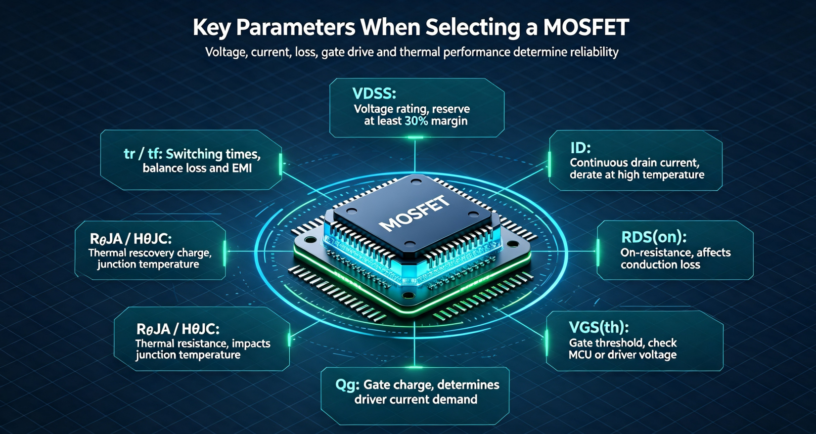
1. Drain-Source Voltage Rating (V₍DSS₎)
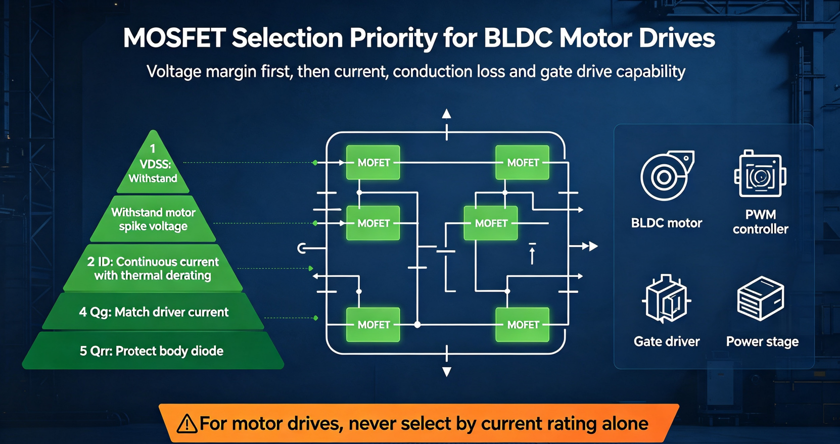
Rule of thumb: Select a VDS with at least 30% voltage margin above the circuit’s maximum operating drain voltage. Voltage spikes from inductive loads (BLDC motors, transformers) will easily break down the device without sufficient margin.
2. Continuous Drain Current (I₍D₎)
Do not only reference the datasheet nominal value: this parameter drops significantly as junction temperature rises. For motor drive and high-power switching applications, reserve a current safety margin of 50% or higher. Pay attention to both DC current and pulsed drain current I₍DM₎ for surge loads.
3. On-Resistance R₍DS(on)₎
Key note: R₍DS(on)₎ rises with increasing junction temperature. For low-voltage high-current BLDC driver solutions, low RDS(on) MOSFETs (Winsok series) effectively reduce thermal stress. Also check test conditions: VGS and current level specified in datasheet.
4. Gate Threshold Voltage V₍GS(th)₎
- Logic-level MOSFET: VGS(th) ~1–2V, suitable for direct driving by MCU IO ports
- Standard power MOSFET: VGS(th) 2–4V, needs dedicated gate driver
Avoid mismatch: If your controller only outputs 3.3V, regular power MOSFETs may not fully turn on.
5. Gate Charge (Qg, Qgs, Qgd)
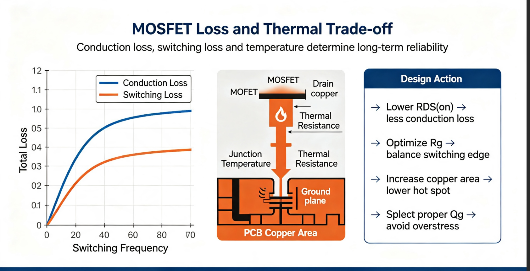
High Qg demands stronger gate drive current; switching loss increases at high frequency. For high-frequency BLDC, DC-DC converters, balance R₍DS(on)₎ and total gate charge to optimize overall power loss. Qgd (Miller charge) is critical for preventing shoot-through in half-bridge circuits.
6. Body Diode Characteristics
Focus on: Reverse recovery charge Qrr. Large Qrr causes severe switching loss and noise in hard-switching topologies. In BLDC three-phase inverters, body diode reverse recovery is a common root cause of device failure. Select fast recovery MOSFETs if external freewheeling diodes are not added.
7. Thermal Parameters
- Maximum junction temperature Tj(max)
- Thermal resistance RθJA / RθJC
These parameters define heat dissipation capability. For SMD MOSFETs, PCB copper area acts as the main heatsink. If the design lacks sufficient copper layout, even devices with high current ratings will overheat.
8. Switching Parameters (tr, tf, td(on), td(off))
Fast switching reduces power loss but generates larger electromagnetic interference. Slow switching lowers noise but increases heat. Match switching speed to your application frequency.
9. Package
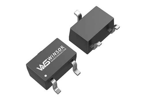
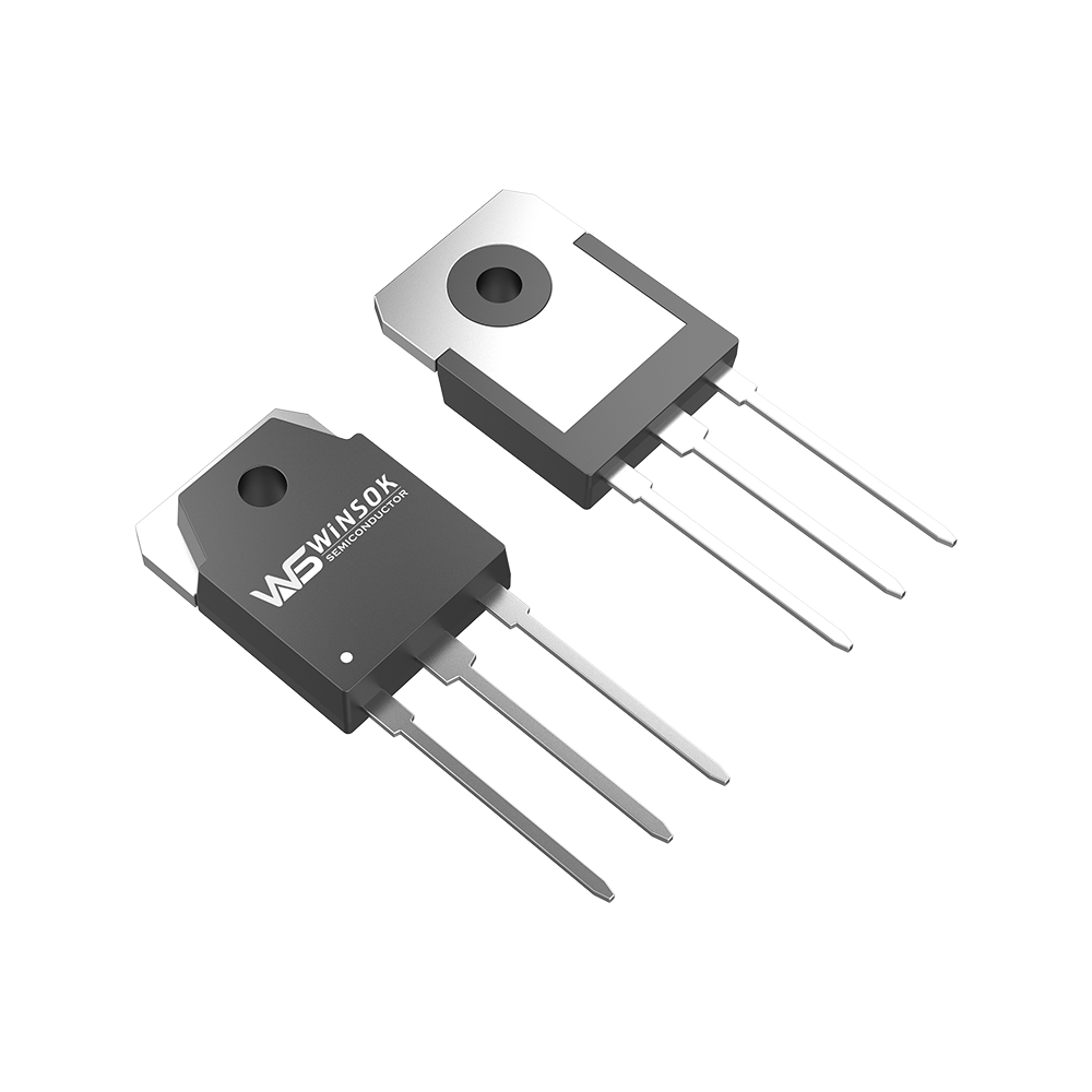
Two core factors: thermal performance and PCB footprint. Small packages limit continuous current due to poor heat dissipation.
Application-Oriented Selection Guidance
BLDC Motor Driver (Our Main Target Market)
Half-bridge topology requires attention to shoot-through risk and body diode reliability.
Low-Voltage DC-DC Converter
High-frequency switching power supply
SiC MOSFET (High voltage high frequency)


-
How Enhanced Package MOSFETs Work
-

About MOSFET driver
-

How to distinguish between P-channel and N-chan...
-

Understanding The Structure of Power MOSFET
-
What is MOSFET?
-
What is the role of small voltage MOSFETs?
-

Do you know the definition of MOSFET?
-

How Much Instantaneous Current Is Required to T...
-

How to Determine nMOSFETs and pMOSFETs
-

Determining MOSFET Threshold Voltage: Expert Te...
-

Do you know about depletion MOSFETs?
-

Special Circuit Design for Power Amplifiers Usi...
-

MOSFET 101: The Ultimate Beginner’s Guide...
-
About the working principle of power MOSFET
-

The role of MOSFETs in circuits
-

How to Evaluate MOSFET Performance Parameters D...


