


1. Comparison of Half-Bridge, Push-Pull and Full-Bridge Inverter Circuits (DC-AC Stage)
1.1 Half-Bridge Inverter
Structure: Consists of 2 MOSFETs and 2 voltage-dividing capacitors. It features a simple circuit and low cost.
Working Principle: The two MOSFETs conduct alternately. The capacitors act as an auxiliary DC bus, generating alternating positive and negative voltages across the load to form AC power.
Features:
- Its voltage utilization rate is half that of a full-bridge circuit, resulting in lower output power under the same input condition.
- Suitable for low-power inverters and low-voltage & low-current applications.
- MOSFETs endure high voltage stress, so it is rarely used in high-voltage and high-power scenarios.
1.2 Push-Pull Inverter
- Structure: Composed of 2 MOSFETs and a center-tapped transformer.
- Working Principle: The two MOSFETs turn on in turn and supply power to two separate windings of the transformer respectively, inducing alternating voltage on the secondary side.
- Features:
Simple drive circuit with built-in isolation via the transformer.
Each MOSFET withstands twice the DC bus voltage, making it vulnerable to breakdown under high voltage.
Prone to transformer magnetic bias. Mainly applied to the front-stage DC-DC boost circuit, and seldom used as a standalone DC-AC inverter.
1.3 Full-Bridge (H-Bridge) Inverter (Mainstream Solution)
- Structure: Equipped with 4 MOSFETs, which work in two diagonal pairs.
- Working Principle: Diagonally paired MOSFETs switch synchronously, enabling bidirectional current flow through the load with the highest voltage utilization efficiency.
- Features:
Covers a wide power range, applicable to both low-power and high-power inverters.
Low voltage requirement for MOSFETs with well-distributed current.
Slightly complicated drive design. It is the standard topology for sine wave inverters.
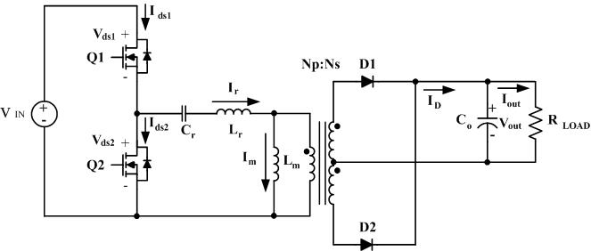
2. Common Causes of MOSFET Damage in Inverters
2.1 Overvoltage Breakdown (Most Common)
- Causes: DC bus voltage surge, back EMF, lightning strike, or voltage spikes caused by load short-circuit. The voltage exceeds the MOSFET’s rated drain-source voltage (\(V_{DSS}\)).
- Symptoms: Permanent short-circuit between drain and source terminals; immediate device burnout or blown fuse once powered on.
- High-risk Scenarios: Startup/shutdown of inductive loads (motors, inductors) and grid backfeed.
2.2 Overcurrent Burnout
- Causes: Output short-circuit, overload, excessive inrush current at power-on; uneven current sharing among parallel-connected MOSFETs leading to overload on individual devices.
- Symptoms: Excessively hot component body, cracking of the device package and burned pins.
2.3 Damage Caused by Abnormal Gate Drive
Causes:
- Insufficient or unstable gate drive voltage makes the MOSFET operate in the linear region, which sharply increases on-resistance and eventually leads to thermal burnout.
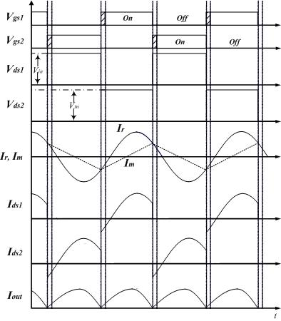
- Insufficient dead time causes shoot-through (simultaneous conduction of upper and lower MOSFETs on the same arm), resulting in direct short-circuit of the DC bus and instantaneous heavy current that burns out the devices.
- Improper selection of gate resistance or electrostatic damage to the gate terminal.
2.4 Thermal Failure from Excessive Switching Loss
Causes: Excessively high switching frequency, mismatched switching speed of MOSFETs generate massive heat during switching; insufficient heat sink or blocked heat dissipation channels.
Symptoms: Continuous overtemperature under full load gradually degrades device performance and eventually causes thermal breakdown.
2.5 Failure of Freewheeling & Snubber Circuits
Causes: Damaged freewheeling diodes or RC snubber circuits fail to clamp voltage spikes generated by inductive loads, leading to repeated impact on MOSFETs.
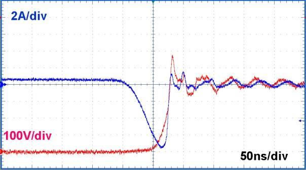
3. Basic Device Selection & Protection Guidelines
- Voltage Rating: Reserve a safety margin of 1.5 ~ 2 times the maximum operating voltage.
- Gate Drive: Set reasonable dead time, adopt matched gate resistors, and connect Zener diodes at the gate to prevent overvoltage.
- Heat Dissipation: Equip high-power designs with adequate heat sinks and thermal grease.
- Surge Protection: Add RC snubbers, varistors and fast recovery diodes to suppress voltage spikes.


-

Advantages of Silicon Carbide (SiC) Power Devices
-

MOSFET Classification Characteristics
-

BJT vs MOSFET: Making the Right Choice for Your...
-

Which brand of MOSFET is good
-

Building the Perfect Ideal Diode with MOSFETs: ...
-

Working principle of N-channel enhancement mode...
-
MOSFET Selection Points
-
Application of MOSFET in the drive circuit of D...
-

Determining MOSFET Threshold Voltage: Expert Te...
-

MPU vs MCU: Key Differences and Applications in...
-
MOSFET small current heating causes and measures
-

Understanding MOSFET Soft Switching: A Comprehe...
-

The Ultimate Guide to Electronic Component Data...
-

Unleashing the Power of MOSFETs and Transistors...
-

What is MOSFET in Electronics: Definition, Work...
-
Understand MOSFET in onearticle


